Skip to content

Patent drawings

Drawing 1 of 4

US 6,760,068

Drawing 1 of 4

Expanded drawing 1 of 4 from US 6,760,068, Correction of corrupted elements in sensors using analog/multi-level non-volatile memory
High-resolution patent drawing

US 6,760,068

Correction of corrupted elements in sensors using analog/multi-level non-volatile memory

Filed
December 31, 1998
Granted
July 6, 2004
Assignee
Sandisk
Inventors
Leo Petropoulos, Sau C. Wong

Abstract

A method and system using a sensor array includes a programmable analog/multi-level memory array for modifying individual outputs from elements in the sensor array in order to obtain a desired sensor array output. The memory array can be programmed with data corresponding to desired modifications, such as low and high offset voltage correction, low gain correction, and gamma correction. Consequently, by utilizing arithmetic circuits, the adverse effects of corrupted elements in a sensor can be corrected by re-programming the memory array with different modification data as the need arises.

View on Google Patents ↗
View Full PatentComplete archived record · 4 figures · 58 description paragraphs · 19 claims

Patent record

Source
Google Patents
Publication
US6760068B2
Application
US09/224,168
Priority
December 31, 1998
Prior art date
December 31, 1998
Publication date
July 6, 2004
Legal status
Expired - Lifetime
Original assignee
SanDisk Corp
Current assignee
SanDisk Technologies LLC
Prior art keywords
sensor, array, voltages, modification, voltage
Source retrieved
July 20, 2026

Classifications

  • HELECTRICITY
  • H04ELECTRIC COMMUNICATION TECHNIQUE
  • H04NPICTORIAL COMMUNICATION, e.g. TELEVISION
  • H04N25/00Circuitry of solid-state image sensors [SSIS]; Control thereof
  • H04N25/60Noise processing, e.g. detecting, correcting, reducing or removing noise
  • H04N25/68Noise processing, e.g. detecting, correcting, reducing or removing noise applied to defects
  • H04N25/69SSIS comprising testing or correcting structures for circuits other than pixel cells

Figures

4 plates

Figure 1 of 4 from US 6,760,068, Correction of corrupted elements in sensors using analog/multi-level non-volatile memory
Figure 01Full resolution ↗
Figure 2 of 4 from US 6,760,068, Correction of corrupted elements in sensors using analog/multi-level non-volatile memory
Figure 02Full resolution ↗
Figure 3 of 4 from US 6,760,068, Correction of corrupted elements in sensors using analog/multi-level non-volatile memory
Figure 03Full resolution ↗
Figure 4 of 4 from US 6,760,068, Correction of corrupted elements in sensors using analog/multi-level non-volatile memory
Figure 04Full resolution ↗

Description

BACKGROUND

1. Field of the Invention

This invention relates to signal sensors, and in particular to correcting corrupted elements in such sensors.

2. Description of Related Art

Several types of sensors exist for capturing data of various signals, such as sound or image signals. These sensors typically sample a portion of the signal and translate that sample into a numerical value. The sum of all the translated samples are then processed to recreate the captured data. An example of a two-dimensional sensor is an image sensor, which converts incident light to voltage levels. Generally, the image is divided up into squares in a grid, with each square in the grid referred to as a pixel or sample. The image at each pixel is sampled by the sensor and translated into a numerical value proportional to the light intensity at the pixel. For color images, the light intensity is measured for each of the three primary colors red, green, and blue. Note that as the size of the pixels decrease and the number of pixels increase for the image, the resolution of the image increases.

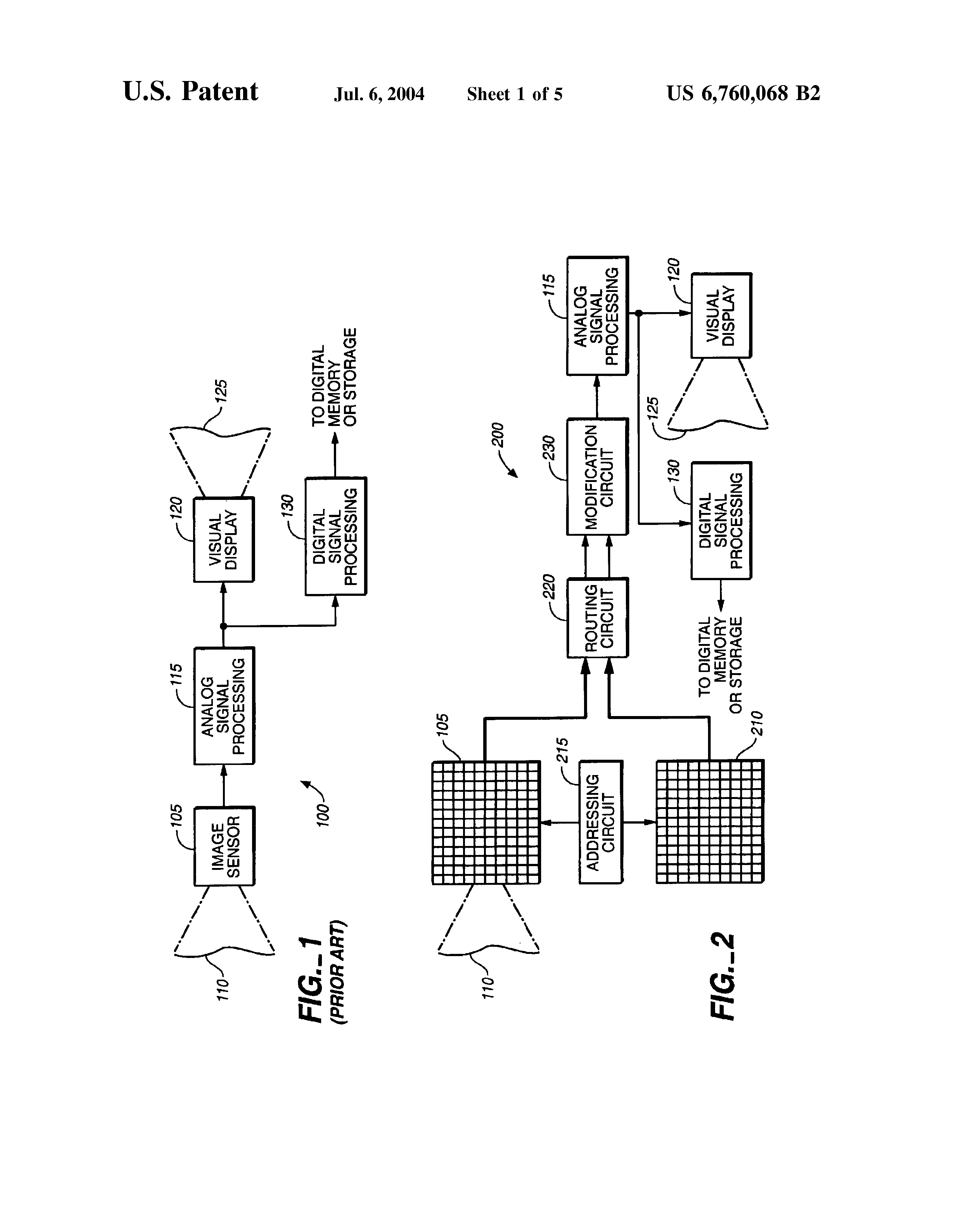
FIG. 1 is a block diagram of a typical imaging system 100 with an image sensor 105. An image 110 is divided up into an array of pixels, with each pixel being sampled by image sensor 105 and then translated into a numerical value. Image sensor 105 can be, for example, a charge-coupled device (CCD), a CMOS device, a vidicon tube, or any other suitable image sensing device which converts the light falling on it from an image into an electrical signal. For example, if image sensor 105 is based on a CCD (such as in a digital camera), the image sensor comprises a chip having an array of photoelectric elements, such as photodiode cells, with each photodiode cell converting an associated pixel to an electrical signal, such as a voltage. As more light falls onto the photodiode cells, more charge accumulates in the cells. The CCD is constructed such that the photodiode cells, which convert the intensity of light into an electric charge, are arranged in a matrix. The electric charge generated in each sensor element is transferred in vertical and horizontal directions, through the CCD array, to the output. After an integration period, the charge is read out from the cells and processed in a suitable analog signal processing circuit 115.

Analog processing circuit 115 processes the captured image from image sensor 105. The processing circuit 115 can include a correlated double sampling (CDS) circuit, a gain adjust circuit, and an offset adjust circuit (all not shown for simplicity) and can be used to perform various functions such as CDS for reduction of low frequency read-out noise from the image sensor and offset of sense amplifiers, color filter array (CFA) interpolation algorithms for color, gamma correction, white balancing, and automatic gain control (AGC) for optimizing the dynamic range of the signal. The processed image signal can then be used for further processing to display a reconstructed image 125 of the original image 110, such as through a visual display 120, which can be a color LCD or a black and white display. The processed analog image signal can also be transmitted to a digital signal processing circuit 130 for conversion to a digital signal, such as with encoding and compression (e.g., according to JPEG). The resulting digital data can then be used or stored in digital memories, such as memory cards.

However, variances across the image sensor can result in a distorted image on display 120 or in the stored memory. If some of the photodiode cells or elements in the image sensor are damaged or have characteristics different from other cells, the weight of the corresponding pixels can be changed in relation to neighboring pixels. The resulting signal from the image sensor thus contains errors, which manifest themselves after signal processing, as a distorted image on the visual display. Depending on the amount of error and the proximity of other varying sensor elements, adverse effects such as “blooming” and “sparkle” can be introduced to the final image.

Variations in the sensor elements are caused by defects during the manufacturing process of the image sensor, as well as normal variations in the manufacturing process. Thus, it is difficult to build a sensor where every sensing element is uniform and perfect. This problem magnifies as the size of the sensor increases and/or the physical size of the sensor elements decreases. In most applications, the quality of the reproduced image is particularly important, especially in high-end imaging applications.

One way of ensuring that faulty or non-comforming sensors are not used is to maintain very tight quality constraints and test criteria before shipping the sensor to the user. Examples of possible types of constraints and criteria include requiring a certain number of sensor elements to meet or exceed a quality threshold or requiring the variance across a portion or portions of the sensor to be smaller than a maximum acceptable value. If a sensor fails to meet these constraints and criteria, that sensor is rejected as having too many bad or inferior sensor elements. Implementing this method requires complex algorithms to test the sensors, which can significantly increase manufacturing and production time, thereby reducing throughput. Furthermore, a large percentage of sensors may be rejected, which increases the cost per yielded sensor. These problems increase as sensor resolutions increase because the probability of having a bad or inferior cell goes up as the number of sensor elements increases and the size of the individual sensor element decreases. Although preventing bad sensors from being shipped to the user, this method does not address errors with the cells after the sensor is shipped, e.g., cell degradation or damage from prolonged use or exposure.

Another method involves measuring the response from each sensor element and mapping all the responses of the sensing elements that have non-conforming responses. This mapping is then used by the sensor manufacturer to map out the errors in the individual elements prior to shipping. In this manner, a faulty sensor is not automatically rejected, but rather, the faulty elements within the sensor are corrected. However, coordinating the transfer of error data for each and every sensor element is difficult. Some vendors address this by using memory embedded with the sensor, which increases the cost and complexity to the sensor. Furthermore, the sensor element response data cannot be updated after the sensor has been shipped, thereby preventing future corrections of the sensor after shipment.

Therefore, an effective method of correcting corrupted sensor element outputs is desired which overcomes the deficiencies as discussed above.

SUMMARY

In accordance with the invention, modification or correction values are stored in a programmable analog/multi-level non-volatile memory array. These values are used to adjust associated outputs from elements of a sensor array for further processing to achieve a desired output. The modification values can be used for a variety of purposes, such as low or high offset voltage correction (by adding or subtracting, respectively, the corresponding modification value), low gain correction (by multiplying the corresponding modification value), or gamma correction (by multiplying the corresponding gamma correction factor) for visual displays.

The analog/multi-level memory array can be erased and re-programmed when modification values need to be changed, e.g., when elements of the sensor array change, such as through time, exposure to the elements, by physical damage, etc. As a result, the output of a sensor array can be maintained at a desired level of quality even as the individual sensor elements change. Furthermore, because errors introduced into sensor output voltages by faulty or non-uniform sensor elements are corrected prior to signal reconstruction, the eventual reconstructed signal is a truer representation of the original signal.

In some embodiments, the memory cells in the memory array have a one-to-one correspondence with the pixel representations from the sensor array. Thus, each output of the sensor array and the corresponding voltage in the memory cell are supplied to a modification circuit for performing the desired modifications. For example, if the desired modifications include correcting for low offset voltages, high offset voltages, low gain, and gamma correction, the modification circuit can include a summing circuit for adding offset voltages stored in a memory array to sensor output voltages, a subtractor circuit for subtracting offset voltages stored in a memory array from sensor output voltages, and an amplifier circuit for multiplying gain voltages and gamma correction voltages stored in memory arrays with sensor output voltages. These circuits can be included separately in the modification circuit or in various combinations of each other.

In other embodiments, the memory array or arrays are smaller in size than the sensor output array. In these embodiments, a decoder is added to the sensor system for determining whether each sensor element output requires modification. When a sensor element needs modification, the decoder determines the address of the memory cell in the memory array corresponding to the sensor element. This corresponding pair is supplied to the modification circuit for performing the desired modification. Sensor outputs not needing modification bypass the modification circuit.

The present invention will be more fully understood upon consideration of the detailed description below, taken together with the accompanying drawings.

BRIEF DESCRIPTION OF THE DRAWINGS

FIG. 1 is a block diagram of a generalized imaging system;

FIG. 2 is a block diagram of an imaging system according to one embodiment of the present invention;

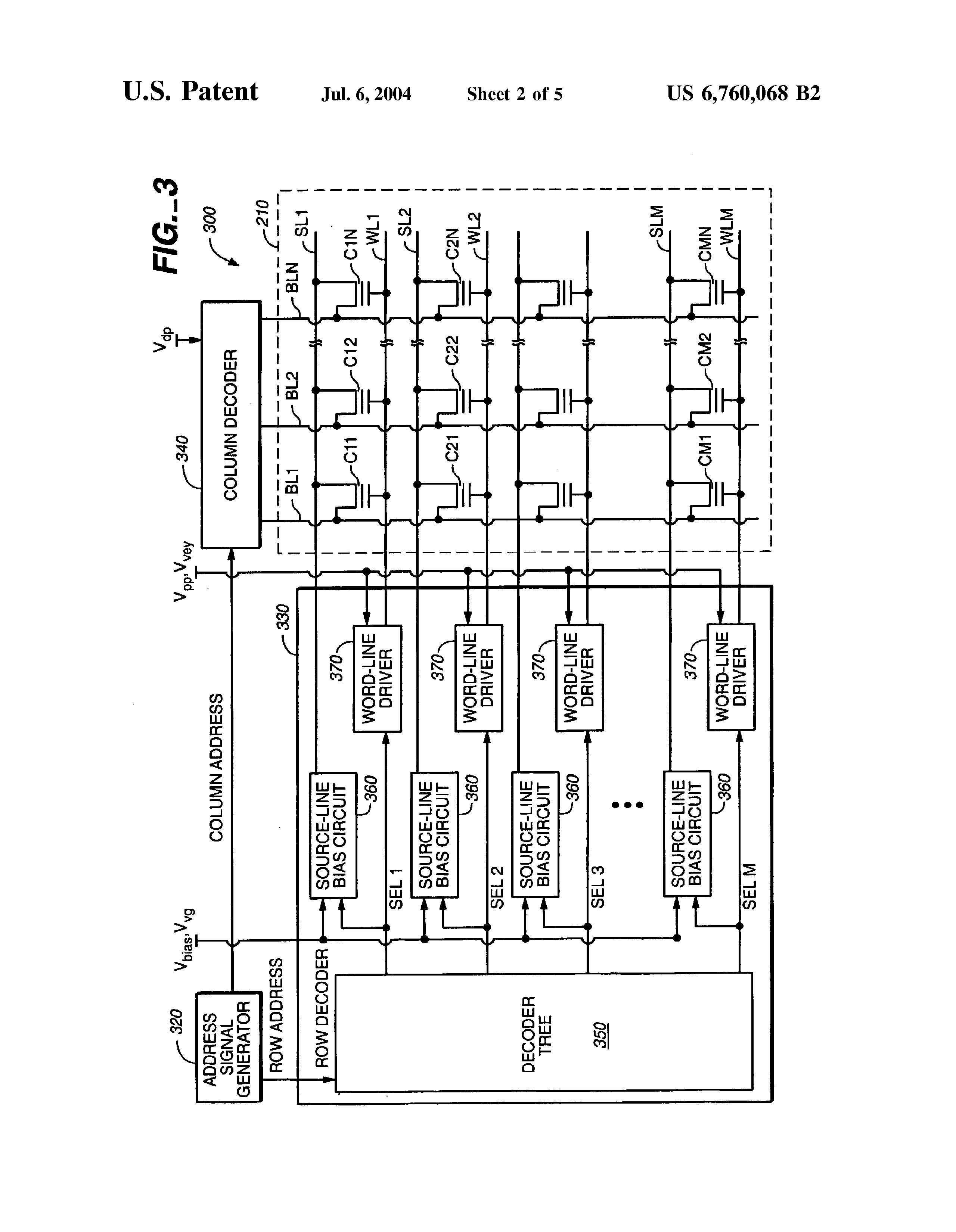
FIG. 3 is diagram of a memory suitable for use with the system of the present invention;

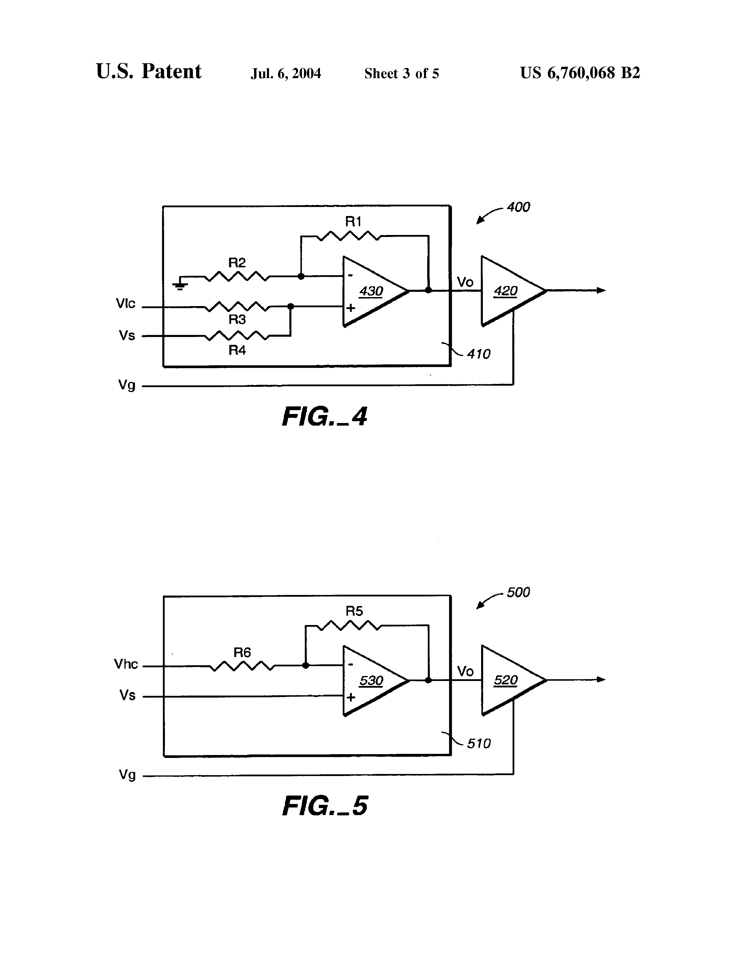
FIG. 4 is a diagram of a modification circuit for correcting low offset voltages according to one embodiment of the present invention;

FIG. 5 is a diagram of a modification circuit for correcting high offset voltages according to one embodiment of the present invention;

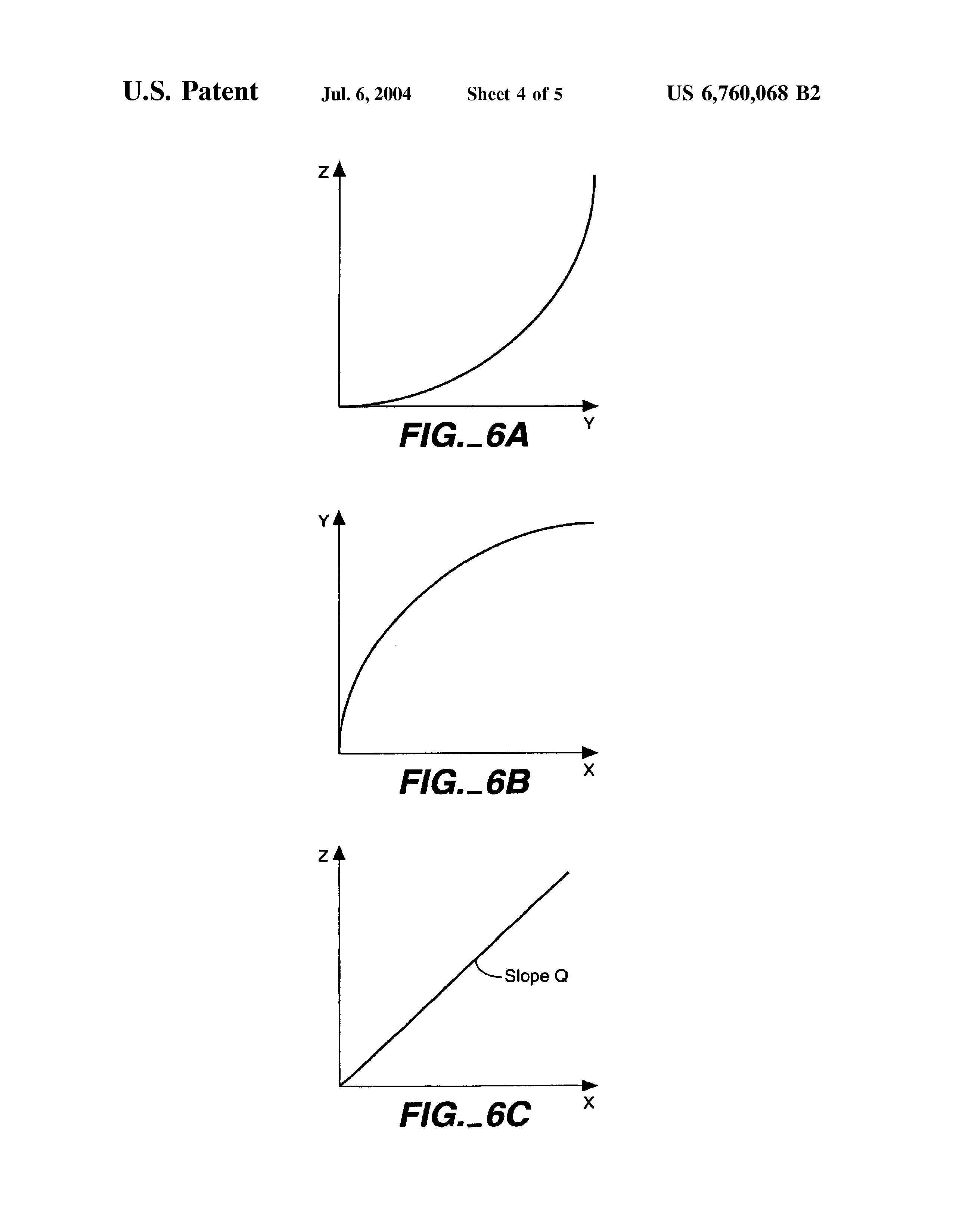
FIGS. 6A, 6B, and 6C are graphs illustrating gamma correction;

FIG. 7 is a diagram of an amplifier for gamma correction; and

FIG. 8 is a block diagram of an imaging system according to another embodiment of the present invention.

Use of the same reference symbols in different figures indicates similar or identical items.

DETAILED DESCRIPTION OF THE PREFERRED EMBODIMENTS

In accordance with the present invention, a method and structure are provided which uses modification or correction values (i.e., voltages) stored in an analog/multi-level memory array to modify the output of a sensor array to obtain a desired result. The memory array can be re-programmed with different modification values for different uses or when elements of the sensor array change. For example, for correcting corrupted elements in a sensor, the memory array can be programmed with appropriate offset voltages to be subtracted or added to the sensor element output or programmed with appropriate gains to be multiplied to sensor elements with low gain. Also, the memory array can be programmed with gamma correction values for gamma correction of visual displays, thereby eliminating the need for a separate gamma correction circuit.

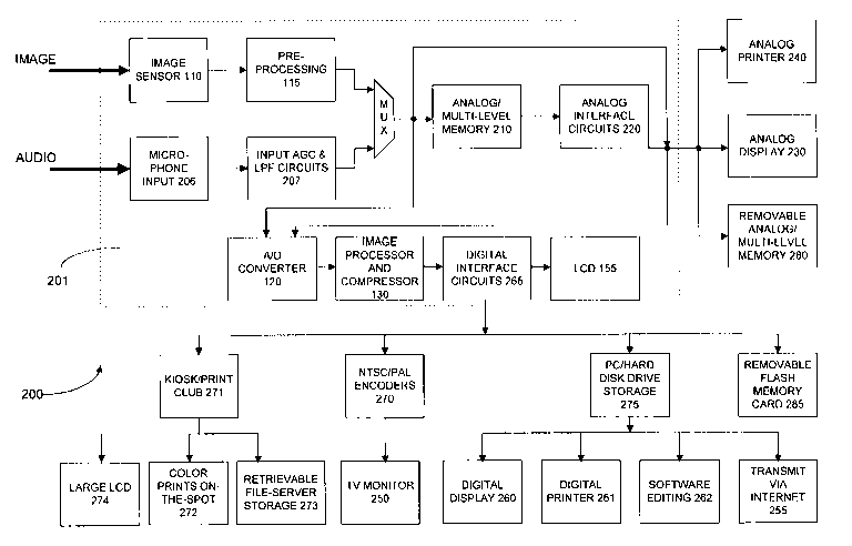
FIG. 2 is a generalized block diagram according to one embodiment of the present invention. One type of sensor, an image sensor 105, is used with an imaging system 200. Image sensor 105 samples an image 110, which has been divided up into an array of pixels. Each cell or sensor element of image sensor 105 samples a corresponding pixel of the image and converts the pixel to a representative voltage. As a result, the image 110 is converted into an array of voltages, as is well known in the art. Pairs of desired corresponding voltages from the array of voltages from image sensor 105 and from the array of voltages stored in an analog/multi-level memory 210 are accessed and read out by an addressing circuit 215. The desired pair or pairs of voltages are then input into a routing circuit 220. Depending on the type of modification, routing circuit 220 routes the two respective voltages from the image sensor and the memory array to the specific circuit (discussed in detail below) in a modification circuitry block 230 for performing the desired modification to the image sensor voltage. Voltages from image sensor elements not requiring modification, i.e., from non-faulty sensor elements, are also input to modification circuitry block 230, but pass through essentially unchanged. Different types of modification include, but are not limited to, adding or subtracting an offset voltage, multiplying a gain voltage, and multiplying a gamma correction voltage.

The modified and any unmodified sensor voltages are supplied to an analog signal processing circuit 115 for processing and eventual display of the reconstructed image 125, such as through a visual display 120. The analog signal from circuit 115 can also be transmitted to a digital signal processing circuit 130, for example, to perform JPEG encoding and compression. The resulting digital signal can then be routed for display, further processing, or storage in a digital memory device, such as an external memory card. Because errors introduced into the image sensor voltages by faulty or non-uniform sensor elements are corrected prior to image reconstruction, the eventual reconstructed image is a truer representation of the original image 110.

The voltages for modifying the sensor element voltages can be programmed and stored in any suitable analog/multi-level memory array 210, such as those described in commonly-owned U.S. Pat. Nos. 5,694,356, entitled “HIGH RESOLUTION ANALOG STORAGE EPROM AND FLASH EPROM” to Wong et al., U.S. Pat. No. 5,680,341, entitled “PIPELINED RECORD AND PLAYBACK FOR ANALOG NON-VOLATILE MEMORY” to Wong et al., and U.S. Pat. No. 5,818,757, entitled “ANALOG AND MULTI-LEVEL MEMORY WITH REDUCED PROGRAM DISTURB” to So et al., and in commonly-owned U.S. patent application Ser. No. 09/159,397, entitled “ANALOG BUFFER MEMORY FOR HIGH SPEED DIGITAL IMAGE CAPTURE” to Wong et al., U.S. Pat. No. 6,594,036, entitled “ANALOG MULTI-LEVEL MEMORY FOR DIGITAL IMAGING” to Wong et al., U.S. Pat. No. 5,923,585, entitled “SOURCE BIASING IN NON-VOLATILE MEMORY HAVING ROW-BASED SECTORS” to Wong et al. and U.S. Pat. No. 5,896,340, entitled “MULTIPLE ARRAY ARCHITECTURE FOR ANALOG OR MULTILEVEL MEMORY” to Wong et al., all of which are incorporated by reference in their entirety.

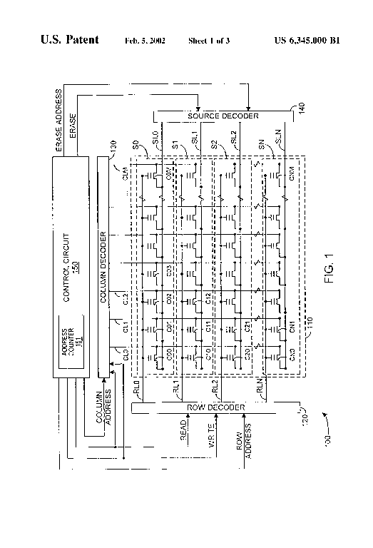
FIG. 3 illustrates a programmable and erasable non-volatile memory 300 with a memory array 210 that can be used in the present invention. Memory array 210 has M rows and N columns of memory cells C11 to CMN. In memory array 210, each memory cell C11 to CMN is a single n-channel floating gate transistor, but other types of memory cells such as split-gate or two-transistor memory cells can also be used. Each memory cell C11 to CMN has a control gate coupled to one of word-lines WL1 to WLM, a drain coupled to one of bit-lines BL1 to BLN, and a source coupled to one of source-lines SL1 to SLM.

When writing a data value, an address signal generator 320 provides address signals indicating a row address and a column address for a selected one of memory cells C11 to CMN to which the data value will be written. The row address identifies the row containing the selected memory cell and a word-line and a source-line coupled to the selected memory cell. The column address identifies the column containing the selected memory cell and a bit-line coupled to the selected memory cell. Address signal generator 320 can be a buffer circuit that generates the address signals from addresses provided by circuitry external to memory 300, or address signal generator 320 can generate sequential addresses for recording analog or multi-level samples of a continuous analog signal.

For an analog/multi-level non-volatile memory, writing a data value to the selected memory cells changes the threshold voltage of the selected memory cell from an erased state to a state indicating the data value being stored. The direction of the change is constant and referred to herein as the programming direction. Programming voltages are applied to the word-line, bit-line, and source-line coupled to the selected memory cell to cause the change in the threshold voltage. For example, to write an analog value to memory cell C11, a row decoder 330 grounds source-line SL1 to a virtual-ground voltage Vvg, which is close to a reference potential Vss and applies a programming voltage Vpp to word-line WL1; and a column decoder 340 applies programming voltage Vdp to bit-line BL1. The magnitudes of the programming voltages Vpp and Vdp depend on structure of memory cells C11 and CMN and may depend on the analog value being written. If memory array 210 is a Flash memory array, typical programming voltages Vpp and Vdp are respectively about 12 volts and about 6 volts above voltage Vss, and the combination of programming voltages causes channel hot electron (CHE) injection that increases the threshold voltage of the selected memory cell.

Column decoder 340 applies programming voltage Vdp to the selected bit-line and disconnects unselected bit-lines. Column decoder 340 can be implemented using designs that are well known in the art.

Row decoder 330 contains a decoder tree 350, source-line bias circuits 360, and word-line drivers 370. Decoder tree 350 generates select signals SEL1 to SELM, each of which corresponds to a row in memory array 210 and indicates whether the corresponding row contains the selected memory cell. Word-line drivers 370 and source-line bias circuits 360 use signals SEL1 and SELM when determining the voltage to be applied to word-lines WL1 to WLM and source-lines SL1 to SLM.

Word-line drivers 370 apply programming and verify voltages Vpp and Vvfy, respectively, to the word-line selected by decoder tree 350 during a write/verify cycle. In alternative embodiments, word-line drivers 370 either ground unselected word-lines or bias some or all of the unselected word-lines at a bias voltage to reduce program disturb. U.S. Pat. No. 5,818,757, entitled “ANALOG AND MULTI-LEVEL MEMORY WITH REDUCED PROGRAM DISTURB”, referenced above, describes word-line drivers that bias word-lines coupled to unselected memory cells that contain data and ground word-lines coupled to unselected memory cells that are erased.

Source-line bias circuits 360 control the voltages on source-lines SL1 to SLM. source-lines SL1 to SLM are electrically isolated from each other, so that each row of memory array 210 constitutes a sector having an independently controllable source voltage. In memory array 210, each sector (or row) can be erased independently of the other sectors when a different type of modification is to be performed on portions of image sensor outputs. Once erased, new modification data can be written to desired memory cells.

During a write to a selected memory cell, the source-line coupled to the selected memory cell is connected to Vss or ground, the source-lines coupled to unselected memory cells are raised to a bias voltage Vbias, the word-line coupled to the selected memory cell is alternating between programming voltage Vpp and verify voltage Vvfy, and the bit-line coupled to the selected memory cell is raised to programming voltage Vdp. Accordingly, desired data or voltages can be programmed and stored in memory array 210 using closed-loop program and verify schemes as described in references incorporated above.

If analog/multi-level memory array 210 is used to correct for low offset voltage in the image sensor cells, then offset voltages are programmed and stored in memory array 210. These offset voltages are added to corresponding low offset voltages from the image sensor. A low offset voltage results in a darker, but accurate, representation of the sampled pixel. Thus, a black level adjustment can be made to the sensor elements with low offset voltage by adding an appropriate offset voltage. The offset voltages to be programmed and stored in memory array 210 can be obtained by exposing all the elements in the image sensor to a light of uniform intensity. For example, the amount of intensity can be of the same order of magnitude as a typical image to be sampled. After image sensor 105 samples the image (the light), each of the sensor elements translates its corresponding pixel to a voltage. Each of these voltages is subtracted from a reference voltage representing the voltage for a perfect sensor element. The resulting array of offset voltages is programmed and stored in memory array 210, which correspond to an individual offset correction voltage for each sensor element. If all the sensor elements are perfect and uniform, the voltages in all the cells in the memory array will be essentially the same magnitude, and the array of offset voltages will be approximately zero. However, if some or all of the sensor elements suffer from a low offset voltage, the corresponding offset voltages in memory array 210 are added to the sensor element read-out voltages to correct the low offset voltage.

FIG. 4 shows a circuit 400, which can be used in modification circuitry block 230, for correcting low offset voltages. Other types of summing circuits can also be used. Circuit 400 includes a summing circuit 410 and an amplifier 420. Summing circuit 410 comprises an operational amplifier (op amp) 430 with four resistors R1 to R4. Resistor R1 is coupled between the inverting input terminal and the output of op amp 430, resistor R2 is coupled between ground and the inverting input terminal of op amp 430, resistor R3 is coupled between the sensor element voltage Vs that routing circuit 220 selected from image sensor 105 and the non-inverting input terminal of op amp 430, and resistor R4 is coupled between the low offset correction voltage Vlc that routing circuit 220 selected from memory array 210 and the non-inverting input terminal of op amp 430. If the resistances of R1 and R2 are equal and the resistances of R3 and R4 are equal, the output Vo of op amp 430 will be the unweighted sum of Vs and Vlc, i.e., Vo=Vs+Vlc.

Other modifications can be made to the sensor element voltages by transmitting different correction voltages from other similar analog/multi-level memory arrays. In FIG. 4, by including amplifier 420, circuit 400 can also make adjustments for gain. The output Vo of summing circuit 410 is coupled to the input of amplifier 420, where the gain of amplifier 420 is determined by the associated voltage Vg from voltages stored in a gain correction analog/multi-level memory array, which is similar to analog/multi-level memory array 210. Gain correction values can be stored in the gain correction memory array using a variety of methods. For example, for an image sensor, a light source can be used to illuminate the sensor. The light source is then linearly ramped from a low intensity to a high intensity, and the individual sensor outputs measured at various times during the ramping. For a uniform and ideal sensor, the output voltages would follow a linear relationship, y=ax+b, where y is the output voltage, x is the input voltage, a is the gain, and b is the offset voltage. By measuring the individual output voltages y and comparing y to the expected value, without the offset, gain correction voltages can be stored in the memory array such that all the sensor elements are corrected to a gain of a. Thus, amplifier 420 can provide a gain less than one, a unity gain, or a gain greater than one to voltage Vo for adjusting the gain of individual sensor elements.

Another analog/multi-level memory array can be used to also correct for high offset voltages in the sensor elements. In this case, offset voltages stored in a high offset correction memory array are subtracted from corresponding sensor element voltages from image sensor 105. The offset voltages are determined in a similar way as described above for correction of low offset voltages, except that the image sensor voltages are subtracted from the reference voltage. FIG. 5 shows a circuit 500, which can also be used in modification block 230, for correcting high offset voltages. Similarly, other types of subtractor circuits are suitable for this invention as well. Circuit 500 includes a subtractor circuit 510 and an amplifier 520. Subtractor circuit 510 subtracts a high offset correction voltage Vhc from the corresponding image sensor voltage Vs. Voltage Vs is supplied to the non-inverting input terminal of an op amp 530. Voltage Vhc is supplied to the inverting input terminal of op amp 530 through a resistor R5, with a resistor R6 coupled between the inverting input terminal and the output Vo of op amp 530. If the resistances of resistors R5 and R6 are equal, then the output voltage Vo is equal to Vs-Vhc. A separate gain correction memory array and amplifier 520 can be included so that gain correction can be made after the high offset voltage correction, similar to the description above.

In addition to correction of high and low offset voltages and gain, an analog/multi-level memory can be used to correct for other factors that can distort a reconstructed image, such as non-linearities in television cameras and monitors or blurry displays of very dark or very light images using gamma correction. Non-linearities are caused when signals are displayed by visual display 120 utilizing a cathode rate tube (CRT) display since CRTs have a non-linear input/output characteristic, as shown in FIG. 6A. The relationship between an input signal voltage (y) to the CRT display and light output (z) from the CRT display can be defined as follows:

z=K*y γ (1)

where z is the light output of the CRT, K is a constant, y is the input signal to the CRT, and γ (gamma) is a constant, typically ranging between 2.2 and 2.5.

Thus, as seen from equation (1) and FIG. 6A, the light output (z) is compressed for low intensity input voltages (y) and expanded for high intensity input voltages (y). As a result, the displayed image on the CRT display is distorted. In order to compensate for this non-linearity of the CRT, an inverse relationship to equation (1) is applied to the input signal (y) before being supplied to the CRT display, known as gamma correction. The gamma correction equation is as follows:

y=C*x 1/γ (2)

where y is the output of gamma correction and the input to the visual display, C is a constant, x is the input to the gamma correction, and 1/γ is the gamma correction factor. Equation (2) is plotted in FIG. 6B.

The combined effect of gamma correction (2) and CRT non-linearity (1) results in a linear output (z), as shown by combining equations (1) and (2) to obtain equation (3), as follows:

z=K*y γ =K*(C*x 1/γ)γ =K*C γ *x=Q*x (3)

where Q is a constant.

Thus, by choosing appropriate values for constants K and C, a linear output z from the visual display 120 can be obtained with a gain Q, as shown in FIG. 6C.

Referring back to FIG. 1, the gamma correction can be performed in analog signal processing circuit 115. However, gamma correction circuitry can be large and complex, with multiple log and anti-log amplifiers, variable gain amplifiers implemented with arrays of precisely matched diodes or with programmable read only memories (PROMs) which have the log and anti-log characteristics stored for look up.

FIG. 7 shows a circuit 700, which can be used in modification block 230, for gamma correction using stored values in an analog/multi-level memory array. Circuit 700 includes an op amp 710, which multiplies the input voltage Vs from individual sensor elements in the image sensor by a corresponding gamma correction factor Vgc stored in the gamma correction memory array. As a result, image sensor elements can be gamma-corrected to produce a linear output from visual display 120 without the need of a separate gamma correction circuit.

By using a plurality of memory arrays 210, each being programmed and stored with voltages for a different modification function, a variety of modifications to the sensor element voltages can be performed. In such a system, a desired one of the memory arrays 210 is selected for a particular modification. The image sensor voltages to be modified and the corresponding voltages in the memory array 210 are read and supplied to the appropriate modification circuit, e.g., such as shown in FIGS. 4, 5, and 7 above, to perform the desired modifications.

In the above embodiments, it was assumed that the size of memory array 210 is the same as that of the image sensor array for a one-to-one correspondence between the memory cells of the array and the pixel voltages in the sensor array, and each associated pair of voltages is supplied to routing circuit 220. However, in many situations, only a few of the image sensor elements may be faulty and in need of correction. In these cases, a smaller sized memory array 810 can be used with a decoder 820, as shown in imaging system 800 of FIG. 8. Memory array 810 is similar to memory array 210 described above, except with less rows and/or columns of memory cells. Voltages from elements of image sensor 105 are input to decoder 820, which decides whether the voltage requires modification, e.g., from a faulty sensor element or for gamma correction. If the voltage requires modification, then decoder 820 accesses the address location of the appropriate memory cell in memory array 810. The voltage from the cell is read and transferred, along with the corresponding voltage from the image sensor element, to routing circuit 220 for modification by the appropriate circuit in modification block 230. Voltages from image sensor elements not requiring modification are passed directly from decoder 820 to analog signal processing circuit 115. The analog signal can then be displayed or transmitted for digital signal processing, as described above.

In other embodiments, a single analog/multi-level memory array can be used in conjunction with a decoder for multiple types of modifications. The memory array is programmed with data corresponding to the desired types of modifications in various portions of the array. The decoder then determines the type of modification for a particular voltage from an image sensor element and accesses the desired voltage from the memory array. Both voltages are then supplied to the appropriate modification circuit.

Because the memory arrays discussed above can be reprogrammed, various types of sensor modifications are possible. Further, as the sensor array changes its response and/or uniformity over time (e.g., due to use degradation, physical damage, etc.), the memory array can be reprogrammed to compensate for the new errors. As a result, the memory array for a sensor can be continually updated in order to maintain the desired output of the sensor.

Although the invention has been described with reference to particular embodiments, the description is only an example of the invention's application and should not be taken as a limitation. For example, the present invention can be applied to any type of one-, two-, or three-dimensional sensor which has individual sensor elements for modification of the sensor element output. Various adaptations and combinations of features of the embodiments disclosed are within the scope of the invention as defined by the following claims.
Claims (19)

  1. A method of processing sensor element outputs in a sensor array, comprising: storing voltages corresponding to a desired modification in a programmable analog/multi-level memory array; and modifying the sensor element outputs with associated ones of the voltages stored in the memory array, wherein said sensor element outputs are multiplied with gamma correction values, wherein the memory array and the sensor array are the same size.
  2. The method of claim 1, further comprising bypassing the modifying for sensor element outputs not needing modification.
  3. A method of processing sensor element outputs in a sensor array, comprising: storing voltages corresponding to a desired modification in a programmable analog/multi-level memory array, wherein each of said voltages is associated with a single one of said sensor elements; and modifying the sensor element outputs with associated ones of the voltages stored in the memory array, wherein the memory array is smaller than the sensor array.
  4. The method of claim 3, further comprising transferring corresponding pairs of sensor element outputs and the voltages stored in the memory array to a modification circuit after said storing.
  5. The method of claim 3, further comprising processing said modified sensor element outputs after said modifying.
  6. The method of claim 3, wherein said sensor array is an image sensor array.
  7. The method of claim 3, wherein said modifying comprises adding one of the voltages stored in the memory array to a corresponding sensor element output, subtracting one of the voltages stored in the memory array from a corresponding sensor element output, or multiplying one of the voltages stored in the memory array with a corresponding sensor element output.
  8. A method of modifying elements in a sensor array, comprising: programming modification voltages in memory cells of an analog/multi-level memory array, wherein the memory array is smaller than the sensor array and wherein each of said modification voltages corresponds with a single one of said sensor elements; reading the modification voltage in the memory cell corresponding to a first voltage from an element in the sensor array requiring modification; supplying the modification voltage and the first voltage to a modification circuit; and modifying the first voltage with the modification voltage, wherein the modification voltages are determined by: exposing sensor elements in a sensor with a known signal; measuring the voltages from the sensor elements; comparing the measured voltages with voltages desired from exposing the sensor elements with the known signal; and performing an arithmetic operation to obtain a modification voltage, wherein the modification voltage modifies a corresponding measured voltage to obtain a desired sensor element voltage.
  9. A signal processing system comprising: a sensor, wherein the sensor outputs voltages forming an array of elements; an analog/multi-level memory array having memory cells corresponding to the array of elements; a modification circuit coupled to the sensor and the memory array, wherein the modification circuit modifies voltages of the array of elements with corresponding voltages of the memory cells, wherein the memory array is smaller than the array of elements; and a decoder circuit coupled to the memory array and the array of elements for determining the memory cell in the memory array corresponding to the voltage from the array of elements requiring modification.
  10. The system of claim 9, wherein the sensor is an image sensor.
  11. The system of claim 9, further comprising a signal processing circuit coupled to the modification circuit for processing modified voltages.
  12. The system of claim 9, wherein the modification circuit comprises a summing circuit.
  13. The system of claim 12, wherein the modification circuit further comprises a subtractor circuit.
  14. The system of claim 13, wherein the modification circuit further comprises a multiplier circuit.
  15. A signal processing, comprising: a sensor, wherein the sensor outputs voltages forming an array of elements; an analog/multi-level memory array having memory cells corresponding to the array of elements; and a modification circuit coupled to the sensor and the memory array, wherein the modification circuit modifies voltages of the array of elements with corresponding voltages of the memory cells, wherein the modification circuit performs gamma correction, wherein the memory array and the array of elements are the same size.
  16. A sensor correction system, comprising: a sensor array having a first plurality of memory cells for storing sensor voltages corresponding to the outputs of the sensor array; a programmable analog/multi-level memory array having a second plurality of memory cells each comprising a source, a drain and a control gate for storing modification voltages corresponding to desired modifications of the sensor voltages, wherein the second plurality of memory cells is smaller than the first plurality of memory cells, wherein each of said modification voltages corresponds with a single one of said sensor elements, and wherein the second plurality of memory cells is arranged in rows and columns in the array; a column decoder having bit-lines coupling the drains of memory cells in each column of the array; a row decoder having word-lines coupling the control gates of memory cells in each row of the array and source-lines coupling the sources of memory cells in each row of the array; a routing circuit coupled to the sensor array and to the programmable analog/multi-level memory array for selecting a first voltage from the sensor array for modification and a corresponding second voltage from the analog/multi-level memory array; and a modification circuit for modifying the first voltage with the second voltage, wherein the first plurality of memory cells is larger in number than the second plurality of memory cells.
  17. The system of claim 16, further comprising an analog signal processing circuit coupled to the modification circuit and a visual display device coupled to the analog signal processing circuit.
  18. The system of claim 17, further comprising a digital signal processing circuit coupled to the analog signal processing circuit.
  19. The system of claim 18, wherein the digital signal processing circuit performs encoding and compression of the signal from the analog signal processing circuit.

Publications

Related applications (3)

  1. US09/224,168

    Priority application

  2. US09/224,168

    Claims priority

  3. US09/224,168

    Patent family

Record timeline

  1. Application filed by SanDisk Corp

  2. Priority to US09/224,168

  3. Assigned to INVOX TECHNOLOGY

  4. Assigned to SANDISK CORPORATION

  5. Publication of US20030090580A1

  6. Application granted

  7. Publication of US6760068B2

  8. Assigned to SANDISK TECHNOLOGIES INC.

  9. Assigned to SANDISK TECHNOLOGIES LLC

  10. Anticipated expiration

  11. Expired - LifetimeCurrent

Legal events

  1. AS

    Assignment

    Owner name: INVOX TECHNOLOGY, CALIFORNIA

    Free format text: ASSIGNMENT OF ASSIGNORS INTEREST;ASSIGNORS:PETROPOULOS, LEO;WONG, SAU C.;REEL/FRAME:010215/0685;SIGNING DATES FROM 19990514 TO 19990827

  2. AS

    Assignment

    Owner name: SANDISK CORPORATION, CALIFORNIA

    Free format text: ASSIGNMENT OF ASSIGNORS INTEREST;ASSIGNOR:INVOX TECHNOLOGY;REEL/FRAME:011812/0888

    Effective date: 19990920

  3. STCF

    Information on status: patent grant

    Free format text: PATENTED CASE

  4. FEPP

    Fee payment procedure

    Free format text: PAT HOLDER NO LONGER CLAIMS SMALL ENTITY STATUS, ENTITY STATUS SET TO UNDISCOUNTED (ORIGINAL EVENT CODE: STOL); ENTITY STATUS OF PATENT OWNER: LARGE ENTITY

  5. FPAY

    Fee payment

    Year of fee payment: 4

  6. REMI

    Maintenance fee reminder mailed

  7. AS

    Assignment

    Owner name: SANDISK TECHNOLOGIES INC., TEXAS

    Free format text: ASSIGNMENT OF ASSIGNORS INTEREST;ASSIGNOR:SANDISK CORPORATION;REEL/FRAME:026224/0738

    Effective date: 20110404

  8. FPAY

    Fee payment

    Year of fee payment: 8

  9. FPAY

    Fee payment

    Year of fee payment: 12

  10. AS

    Assignment

    Owner name: SANDISK TECHNOLOGIES LLC, TEXAS

    Free format text: CHANGE OF NAME;ASSIGNOR:SANDISK TECHNOLOGIES INC;REEL/FRAME:038813/0004

    Effective date: 20160516

Patent citations (58)

  1. US5619445A

    Analog memory system having a frequency domain transform processor

    Hyatt; Gilbert P. · April 8, 1997

  2. US5339275A

    Analog memory system

    Hyatt Gilbert P · August 16, 1994

  3. US3719922A

    Digital camera

    L Lopes · March 6, 1973

  4. US4057830A

    Electronic photography system

    Texas Instruments Incorporated · November 8, 1977

  5. US3927308A

    Monitor and results computer system

    Ebasco Serv · December 16, 1975

  6. US4038685A

    Apparatus for automatic gamma control of television color signals

    Rca Corporation · July 26, 1977 · Examiner cited

  7. US4131919A

    Electronic still camera

    Eastman Kodak Company · December 26, 1978

  8. US4445189A

    Analog memory for storing digital information

    Hyatt Gilbert P · April 24, 1984

  9. US4420773A

    Electronic photographic camera

    Nippon Kogaku K.K. · December 13, 1983

  10. US4456931A

    Electronic camera

    Nippon Kogaku K.K. · June 26, 1984

  11. US4614966A

    Electronic still camera for generating long time exposure by adding results of multiple short time exposures

    Olympus Optical Co., Ltd. · September 30, 1986

  12. US4602291A

    Pixel non-uniformity correction system

    Xerox Corporation · July 22, 1986 · Examiner cited

  13. US4803554A

    Electronic imaging camera utilizing EPROM memory

    Polaroid Corporation · February 7, 1989

  14. US4875098A

    Output signal processing circuit for CCD register

    Sony Corporation · October 17, 1989 · Examiner cited

  15. US5034804A

    Electronic still camera with various modes of data compression

    Kabushiki Kaisha Toshiba · July 23, 1991

  16. US4989179A

    High density integrated circuit analog signal recording and playback system

    Information Storage Devices, Inc. · January 29, 1991

  17. US5155584A

    Image recording reproducing apparatus switching image sensor signals or reproduced signals to an A/D converter

    Canon Kabushiki Kaisha · October 13, 1992

  18. US5280358A

    Photoelectric converting apparatus having an analog memory

    Canon Kabushiki Kaisha · January 18, 1994

  19. US5055930A

    Image sensing and recording device having a multilayer analog memory stacked on an image sensing array

    Olympus Optical Co., Ltd. · October 8, 1991

  20. US5049983A

    Digital camera apparatus having an analog emphasis circuitry

    Sony Corporation · September 17, 1991

  21. US5264944A

    Multi-function digital CCD camera

    Kabushiki Kaisha Toshiba · November 23, 1993

  22. US5047861A

    Method and apparatus for pixel non-uniformity correction

    Eastman Kodak Company · September 10, 1991 · Examiner cited

  23. US5274457A

    Digital electronic still camera having removable record means

    Sony Corporation · December 28, 1993

  24. US5519654A

    Semiconductor memory device with external capacitor to charge pump in an EEPROM circuit

    Kabushiki Kaisha Toshiba · May 21, 1996

  25. US5164915A

    Cascading analog record/playback devices

    Information Storage Devices, Inc. · November 17, 1992

  26. US5576757A

    Electronic still video camera with direct personal computer (PC) compatible digital format output

    St. Clair Intellectual Property Consultants, Inc. · November 19, 1996

  27. US5295077A

    Digital electronic still camera

    Ricoh Company, Ltd. · March 15, 1994

  28. US5317407A

    Fixed-pattern noise correction circuitry for solid-state imager

    General Electric Company · May 31, 1994 · Examiner cited

  29. US5272535A

    Image sensor with exposure control, selectable interlaced, pseudo interlaced or non-interlaced readout and video compression

    Loral Fairchild Corporation · December 21, 1993 · Examiner cited

  30. US5289286A

    Solid state sensor having logarithmic photovoltaic response, with pixel uniformity correction and white balance circuitry therefor

    Minolta Camera Kabushiki Kaisha · February 22, 1994 · Examiner cited

  31. US5585846A

    Image signal processing circuit in a digital camera having gain and gamma control

    Samsung Electronics Co., Ltd. · December 17, 1996

  32. US5295485A

    Ultrasonic diagnostic system

    Hitachi, Ltd. · March 22, 1994

  33. US5910913A

    Non-volatile semiconductor memory

    Hitachi, Ltd. · June 8, 1999 · Examiner cited

  34. JPH0636578A

    Eeprom

    Sony Corp · February 10, 1994

  35. US5541653A

    Method and appartus for increasing resolution of digital color images using correlated decoding

    Sri International · July 30, 1996

  36. US5739850A

    Apparatus for improving the image and sound processing capabilities of a camera

    Canon Kabushiki Kaisha · April 14, 1998 · Examiner cited

  37. US5687115A

    Write circuits for analog memory

    Invoice Technology, Inc. · November 11, 1997

  38. US5644636A

    Method and apparatus for securing data stored in semiconductor memory cells

    Xtec, Incorporated · July 1, 1997

  39. US5606365A

    Interactive camera for network processing of captured images

    Eastman Kodak Company · February 25, 1997

  40. US5745409A

    Non-volatile memory with analog and digital interface and storage

    Invox Technology · April 28, 1998

  41. US20010010551A1

    Circuit, pixel, device and method for reducing fixed pattern noise in solid state imaging devices

    Bart Dierickx · August 2, 2001 · Examiner cited

  42. US5680341A

    Pipelined record and playback for analog non-volatile memory

    Invoice Technology · October 21, 1997

  43. EP0798739A2

    Read circuit which uses a coarse-to-fine search when reading the threshold voltage of a memory cell

    INVOX Technology · October 1, 1997 · Examiner cited

  44. US5777923A

    Flash memory read/write controller

    Aplus Integrated Circuits, Inc. · July 7, 1998

  45. US6282462B1

    Image acquisition system

    Metrovideo Inc. · August 28, 2001 · Examiner cited

  46. US5818757A

    Analog and multi-level memory with reduced program disturb

    Invox Technology · October 6, 1998

  47. US5760727A

    Method for synchronizing scanning speed and data transmission speed of a scanner

    Primax Electronics Ltd. · June 2, 1998

  48. US6433823B1

    Solid state image sensing device and image sensing method

    Minolta Co., Ltd. · August 13, 2002 · Examiner cited

  49. US6177956B1

    System and method for correlating processing data and image data within a digital camera device

    Flashpoint Technology, Inc. · January 23, 2001

  50. US6175937B1

    Apparatus and method for programming multistate memory device

    Micron Technology, Inc. · January 16, 2001

  51. US5867430A

    Bank architecture for a non-volatile memory enabling simultaneous reading and writing

    Advanced Micro Devices Inc · February 2, 1999

  52. US5901086A

    Pipelined fast-access floating gate memory architecture and method of operation

    Motorola, Inc. · May 4, 1999

  53. US5923585A

    Source biasing in non-volatile memory having row-based sectors

    Invox Technology · July 13, 1999 · Examiner cited

  54. USD389501S

    Digital camera

    Intel Corporation · January 20, 1998

  55. US6487116B2

    Precision programming of nonvolatile memory cells

    Silicon Storage Technology, Inc. · November 26, 2002 · Examiner cited

  56. US6104437A

    Display signal processing device having a controllable LED display

    Matsushita Electric Industrial Co., Ltd. · August 15, 2000 · Examiner cited

  57. US6134145A

    High data rate write process for non-volatile flash memories

    Sandisk Corporation · October 17, 2000

  58. US5969986A

    High-bandwidth read and write architectures for non-volatile memories

    Invox Technology · October 19, 1999

Cited by (70)

  1. US7518910B2

    Variable reading of non-volatile memory

    Sandisk Corporation · April 14, 2009

  2. US7020017B2

    Variable programming of non-volatile memory

    Sandisk Corporation · March 28, 2006

  3. US20060098483A1

    Variable programming of non-volatile memory

    Jian Chen · May 11, 2006 · Examiner cited

  4. US20060133138A1

    Systems for variable programming of non-volatile memory

    Jian Chen · June 22, 2006 · Examiner cited

  5. US7259987B2

    Systems for variable programming of non-volatile memory

    Sandisk Corporation · August 21, 2007

  6. US7489542B2

    Systems for variable reading in non-volatile memory

    Sandisk Corporation · February 10, 2009

  7. US20050219896A1

    Variable programming of non-volatile memory

    Jian Chen · October 6, 2005 · Examiner cited

  8. US20070247916A1

    Systems for Variable Reading in Non-Volatile Memory

    Jian Chen · October 25, 2007 · Examiner cited

  9. US20090213250A1

    Internal Storage of Camera Characteristics During Production

    Nokia Corporation · August 27, 2009 · Examiner cited

  10. US20070206421A1

    Read operation for non-volatile storage with compensation for coupling

    Nima Mokhlesi · September 6, 2007 · Examiner cited

  11. US20110141810A1

    Read operation for non-volatile storage with compensation for coupling

    Nima Mokhlesi · June 16, 2011 · Examiner cited

  12. US8427873B2

    Read operation for non-volatile storage with compensation for coupling

    Sandisk Technologies Inc. · April 23, 2013

  13. USRE46279E1

    Read operation for non-volatile storage with compensation for coupling

    Sandisk Technologies Llc · January 17, 2017

  14. US7499319B2

    Read operation for non-volatile storage with compensation for coupling

    Sandisk Corporation · March 3, 2009

  15. US8199571B2

    Read operation for non-volatile storage with compensation for coupling

    Sandisk Technologies Inc. · June 12, 2012

  16. US20110225473A1

    Read operation for non-volatile storage with compensation for coupling

    Nima Mokhlesi · September 15, 2011 · Examiner cited

  17. US20090129159A1

    Read operation for non-volatile storage with compensation for coupling

    Nima Mokhlesi · May 21, 2009 · Examiner cited

  18. US7613068B2

    Read operation for non-volatile storage with compensation for coupling

    Sandisk Corporation · November 3, 2009

  19. US20090129160A1

    Read operation for non-volatile storage with compensation for coupling

    Nima Mokhlesi · May 21, 2009 · Examiner cited

  20. US7911838B2

    Read operation for non-volatile storage with compensation for coupling

    Sandisk Corporation · March 22, 2011

  21. US20070206426A1

    System for performing read operation on non-volatile storage with compensation for coupling

    Nima Mokhlesi · September 6, 2007 · Examiner cited

  22. US20100074018A1

    Read operation for non-volatile storage with compensation for coupling

    Nima Mokhlesi · March 25, 2010 · Examiner cited

  23. US7436733B2

    System for performing read operation on non-volatile storage with compensation for coupling

    Sandisk Corporation · October 14, 2008

  24. US7778106B2

    Read operation for non-volatile storage with compensation for coupling

    Sandisk Corporation · August 17, 2010

  25. US20110134693A1

    Apparatus for reducing the impact of program disturb

    Gerrit Jan Hemink · June 9, 2011 · Examiner cited

  26. US7796433B2

    Apparatus for reducing the impact of program disturb

    Sandisk Corporation · September 14, 2010

  27. US7911846B2

    Apparatus for reducing the impact of program disturb

    Sandisk Corporation · March 22, 2011

  28. US20100188897A1

    Apparatus for reducing the impact of program disturb

    Gerrit Jan Hemink · July 29, 2010 · Examiner cited

  29. US7436713B2

    Reducing the impact of program disturb

    Sandisk Corporation · October 14, 2008

  30. US7426137B2

    Apparatus for reducing the impact of program disturb during read

    Sandisk Corporation · September 16, 2008

  31. US20110134699A1

    Apparatus for reducing the impact of program disturb

    Gerrit Jan Hemink · June 9, 2011 · Examiner cited

  32. US7499326B2

    Apparatus for reducing the impact of program disturb

    Sandisk Corporation · March 3, 2009

  33. US8270217B2

    Apparatus for reducing the impact of program disturb

    Sandisk Technologies Inc. · September 18, 2012

  34. US7515463B2

    Reducing the impact of program disturb during read

    Sandisk Corporation · April 7, 2009

  35. US8331154B2

    Apparatus for reducing the impact of program disturb

    Sandisk Technologies Inc. · December 11, 2012

  36. US8542530B2

    Apparatus for reducing the impact of program disturb

    Sandisk Technologies Inc. · September 24, 2013

  37. US20090175078A1

    Apparatus for reducing the impact of program disturb

    Gerrit Jan Hemink · July 9, 2009 · Examiner cited

  38. US8593871B2

    Apparatus for reducing the impact of program disturb

    Sandisk Technologies Inc. · November 26, 2013

  39. US7843739B2

    System for verifying non-volatile storage using different voltages

    Sandisk Corporation · November 30, 2010

  40. US20080316829A1

    System for verifying non-volatile storage using different voltages

    Gerrit Jan Hemink · December 25, 2008 · Examiner cited

  41. US20070279993A1

    Verify operation for non-volatile storage using different voltages

    Gerrit Jan Hemink · December 6, 2007 · Examiner cited

  42. US20070279985A1

    System for verifying non-volatile storage using different voltages

    Gerrit Jan Hemink · December 6, 2007 · Examiner cited

  43. US8014205B2

    System for verifying non-volatile storage using different voltages

    Sandisk Technologies Inc. · September 6, 2011

  44. US20110032769A1

    System for verifying non-volatile storage using different voltages

    Gerrit Jan Hemink · February 10, 2011 · Examiner cited

  45. US7440331B2

    Verify operation for non-volatile storage using different voltages

    Sandisk Corporation · October 21, 2008

  46. US7457163B2

    System for verifying non-volatile storage using different voltages

    Sandisk Corporation · November 25, 2008

  47. US20080056001A1

    System for performing data pattern sensitivity compensation using different voltage

    Nima Mokhlesi · March 6, 2008 · Examiner cited

  48. US20080056000A1

    System for performing data pattern sensitivity compensation using different voltage

    Nima Mokhlesi · March 6, 2008 · Examiner cited

  49. US7450421B2

    Data pattern sensitivity compensation using different voltage

    Sandisk Corporation · November 11, 2008

  50. US7561473B2

    System for performing data pattern sensitivity compensation using different voltage

    Sandisk Corporation · July 14, 2009

  51. US20070279995A1

    System for performing data pattern sensitivity compensation using different voltage

    Nima Mokhlesi · December 6, 2007 · Examiner cited

  52. US20070279994A1

    Data pattern sensitivity compensation using different voltage

    Nima Mokhlesi · December 6, 2007 · Examiner cited

  53. US7310272B1

    System for performing data pattern sensitivity compensation using different voltage

    Sandisk Corporation · December 18, 2007

  54. US7590002B2

    Resistance sensing and compensation for non-volatile storage

    Sandisk Corporation · September 15, 2009

  55. US7518923B2

    Margined neighbor reading for non-volatile memory read operations including coupling compensation

    Sandisk Corporation · April 14, 2009

  56. US20080158946A1

    Alternating read mode

    Nima Mokhlesi · July 3, 2008 · Examiner cited

  57. US20080158967A1

    Resistance sensing and compensation for non-volatile storage

    Nima Mokhlesi · July 3, 2008 · Examiner cited

  58. US7616498B2

    Non-volatile storage system with resistance sensing and compensation

    Sandisk Corporation · November 10, 2009

  59. US20080158974A1

    Apparatus with alternating read mode

    Nima Mokhlesi · July 3, 2008 · Examiner cited

  60. US20080158985A1

    Systems for margined neighbor reading for non-volatile memory read operations including coupling compensation

    Nima Mokhlesi · July 3, 2008 · Examiner cited

  61. US7495962B2

    Alternating read mode

    Sandisk Corporation · February 24, 2009

  62. US7440324B2

    Apparatus with alternating read mode

    Sandisk Corporation · October 21, 2008

  63. US20080158983A1

    Non-volatile storage system with resistance sensing and compensation

    Nima Mokhlesi · July 3, 2008 · Examiner cited

  64. US7606070B2

    Systems for margined neighbor reading for non-volatile memory read operations including coupling compensation

    Sandisk Corporation · October 20, 2009

  65. US7535764B2

    Adjusting resistance of non-volatile memory using dummy memory cells

    Sandisk Corporation · May 19, 2009

  66. US20080273388A1

    Adjusting resistance of non-volatile memory using dummy memory cells

    Henry Chin · November 6, 2008 · Examiner cited

  67. US9459599B2

    Dynamic adjustment of operational parameters to compensate for sensor based measurements of circuit degradation

    International Business Machines Corporation · October 4, 2016

  68. US9465373B2

    Dynamic adjustment of operational parameters to compensate for sensor based measurements of circuit degradation

    International Business Machines Corporation · October 11, 2016

  69. US20170083749A1

    Array sensor and sensing method thereof

    Egis Technology Inc. · March 23, 2017 · Examiner cited

  70. US10282578B2

    Array sensor and sensing method thereof

    Egis Technology Inc. · May 7, 2019 · Examiner cited

Related Patents