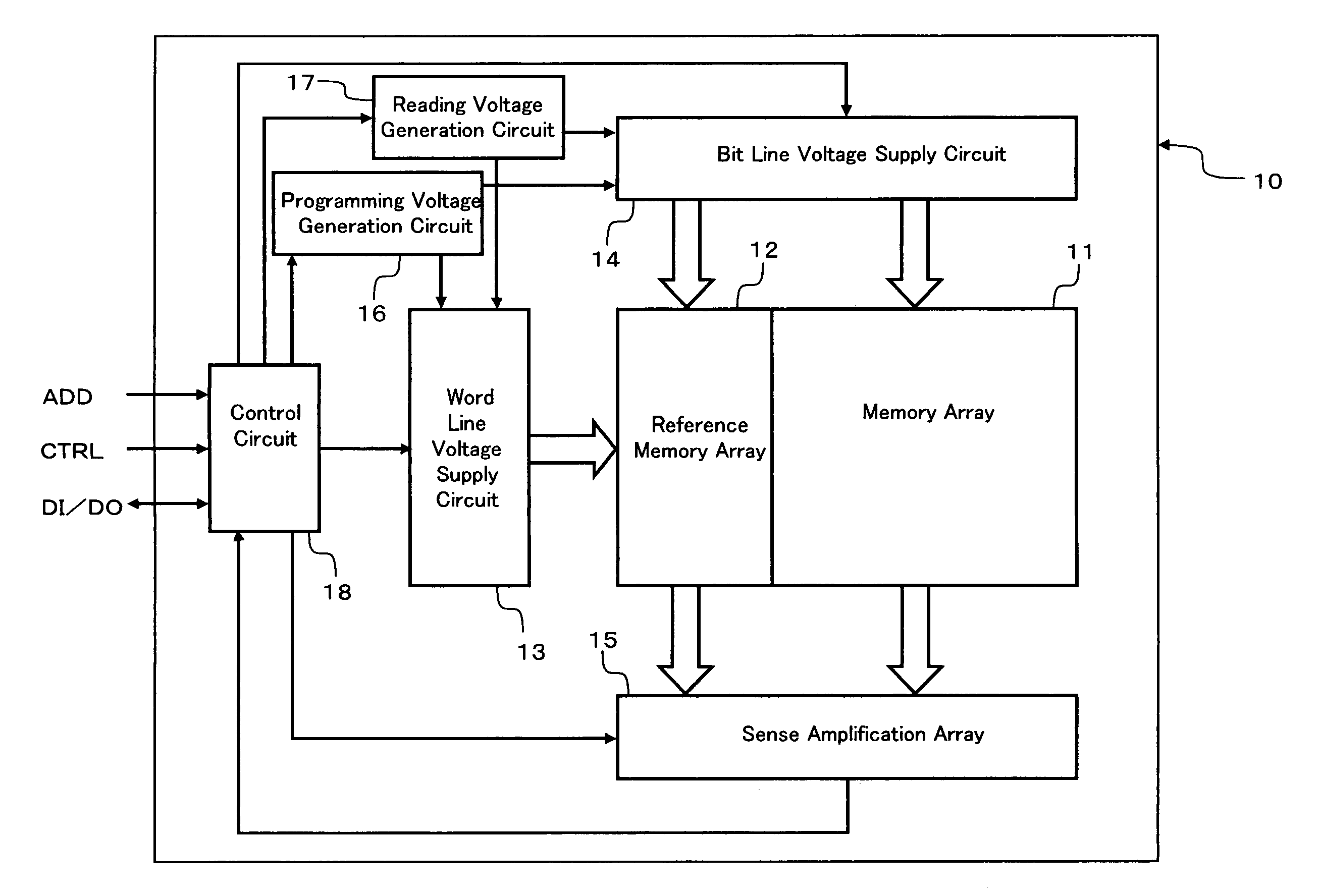
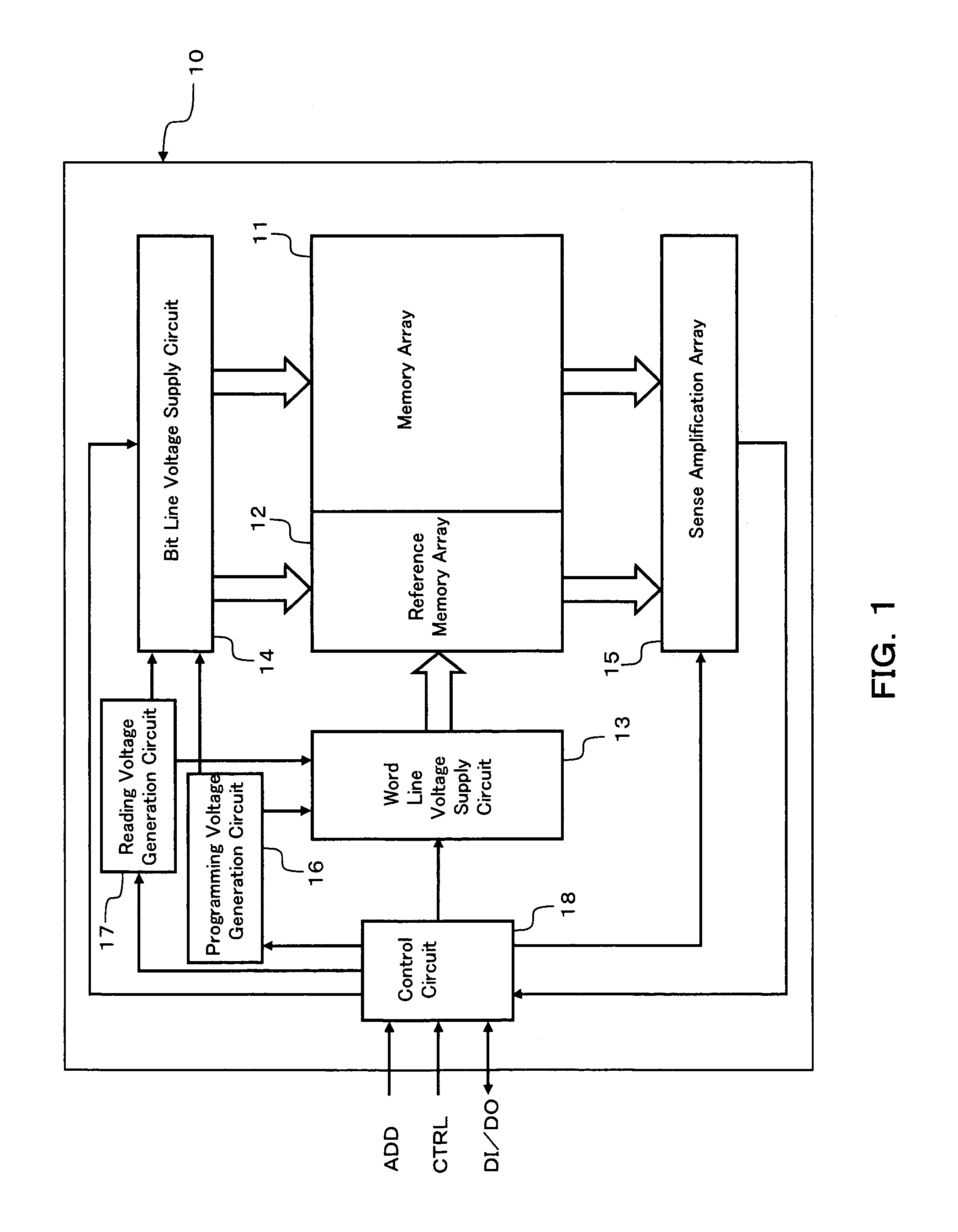
Exemplary embodiments of a nonvolatile semiconductor memory device according to the present invention will be explained below with reference to the accompanying drawings. FIG. 1 is a functional block configuration diagram of a memory device 10 according to the present invention. Peripheral circuits including input circuits of address input signals (ADD in FIG. 1), data input signals (DI in FIG. 1) and control signals (CTRL in FIG. 1), output circuits of data output signals (DO in FIG. 1), and a decoder circuit of the address input signals have details similar to those in a known nonvolatile semiconductor memory device like a flash memory. Therefore, the description of these circuits will be omitted. FIG. 1 mainly illustrates a circuit portion concerning the program operation of a memory array 11 of the memory device 10.
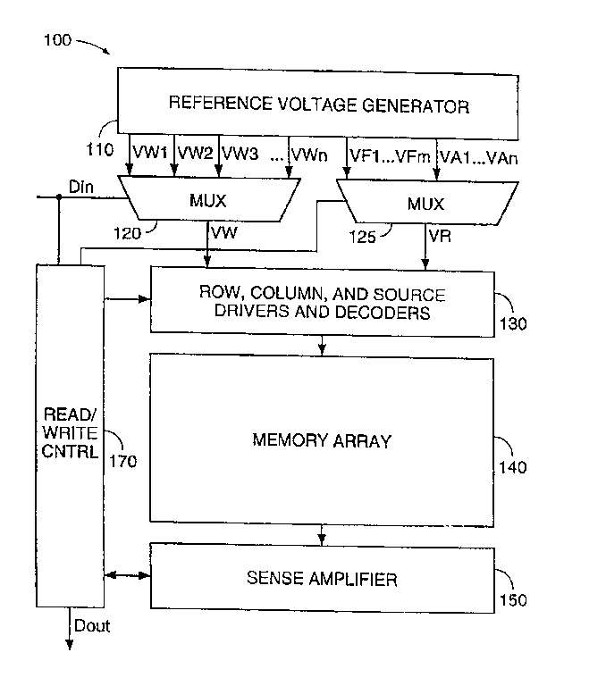
As shown in FIG. 1, the memory device 10 according to the present invention comprises: the memory array 11; a reference memory array 12; a word line voltage supply circuit 13 that supplies a word line voltage to the word lines of the memory array 11 and the reference memory array 12; a bit line voltage supply circuit 14 that supplies a bit line voltage to the bit lines of the memory array 11 and the reference memory array 12; a sense amplification array 15 consisting of a plurality of sense amplifiers each of which compares a read voltage read out from a selected bit line of the memory array 11 with a reference voltage read out from a selected bit line of the reference memory array 12, thereby to verify programming states of a plurality of selected memory cells of the memory array 11; a programming voltage generation circuit 16 that generates a programming gate voltage supplied as a word line voltage, and a programming drain voltage supplied as a bit line voltage, during a programming process; a reading voltage generation circuit 17 that generates a verification gate voltage supplied as a word line voltage, and a verification drain voltage supplied as a bit line voltage, during a verification process; and a control circuit 18 that controls the operation of the circuits 13 to 17, respectively.
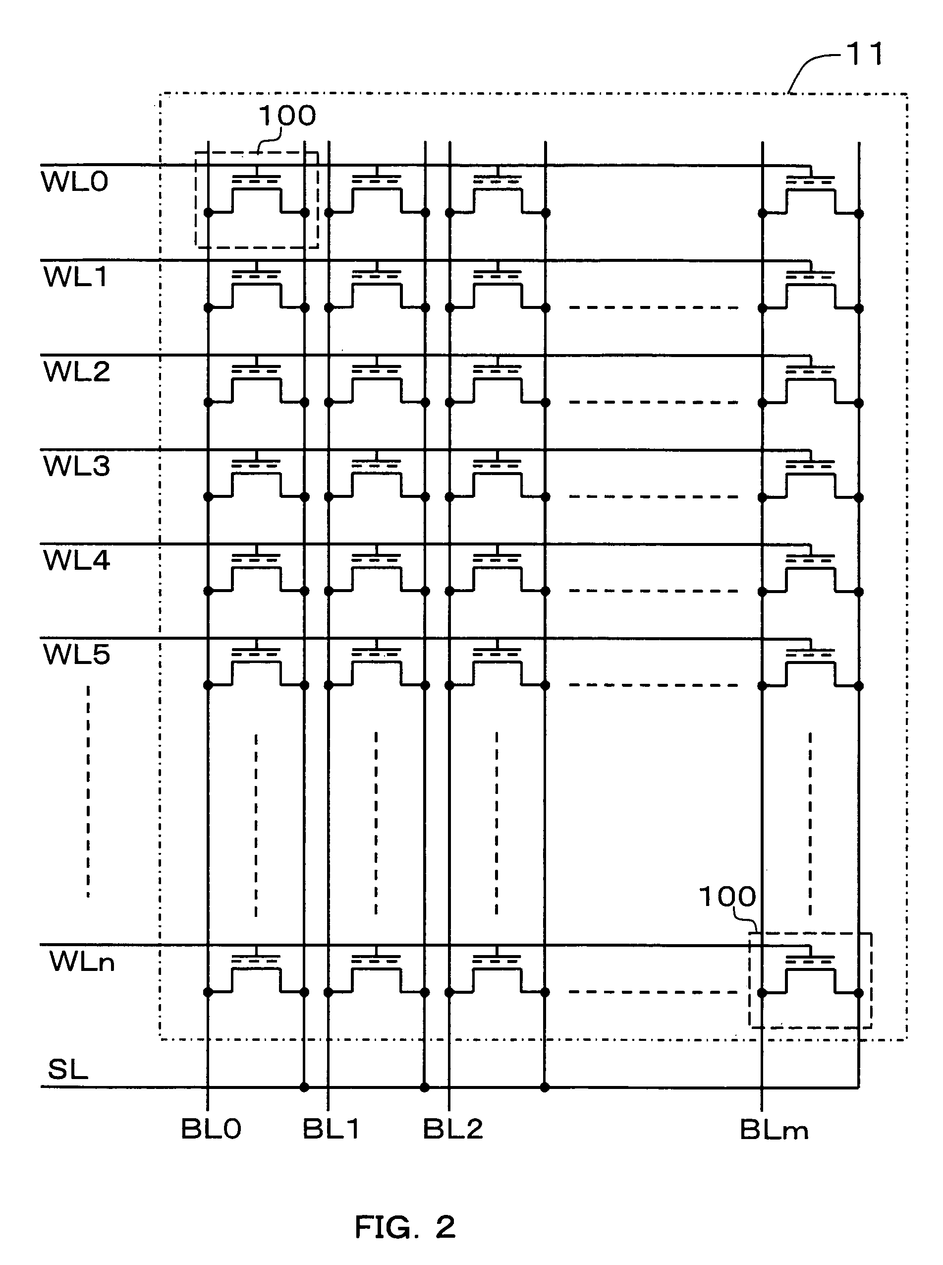
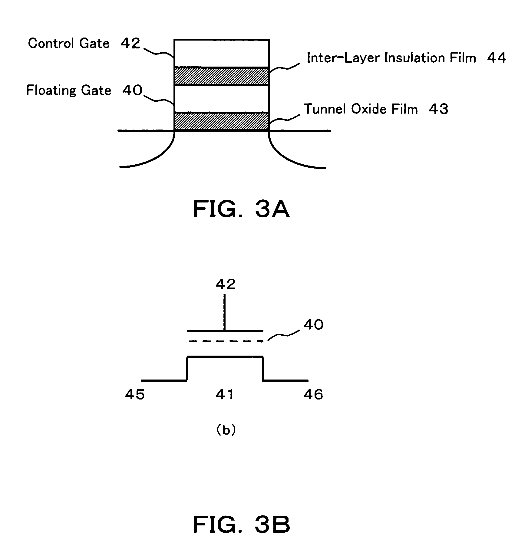
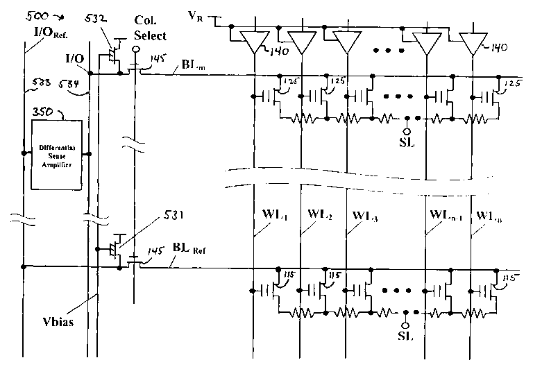
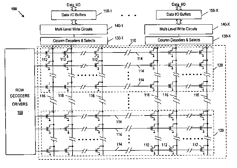
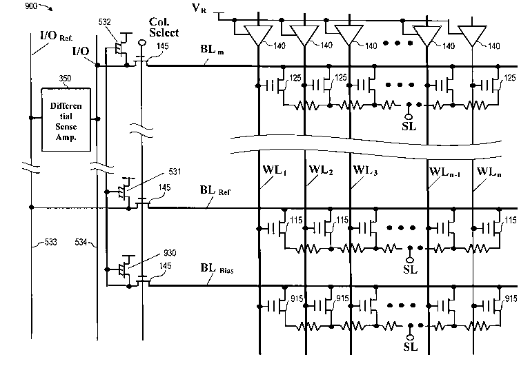
As shown in FIG. 2, the memory array 11 has a plurality of memory cells 100 arranged in a row direction and a column direction, respectively. A plurality of control gates of the memory cells 100 in the same row are mutually connected to form common word lines WL0 to WLn, and a plurality of drains of the memory cells 100 in the same column are mutually connected to form common bit lines BL0 to BLm. Sources of the memory cells 100 are mutually connected to form a common source line SL. User data are stored in the memory array 11. As shown in FIGS. 3A and 3B, the memory cell 100 has a transistor structure that is similar to a floating gate type flash memory cell such as the conventional ETOX type flash memory. This transistor structure has a floating gate 40 formed between the channel area 41 and the control gate 42 via the insulation films 43 and 44. The memory cell 100 can take three or more memory states including two or more programming states corresponding to a threshold voltage level of a transistor determined according to the charge of the floating gate 40.
The reference memory array 12 also has, similar to the memory array 11, a structure having the flash memory cells 100 arranged in an array shape as shown in FIG. 2. The reference memory array 12 supplies a reference voltage to the sense amplifiers in the verification of the program operation and the normal array read operation. The word lines common to the memory array 11 are used to prevent the read margin from being degraded. Predetermined threshold voltages are set (i.e., programmed) to the memory cells 100 of each column of the reference memory array 12 for specific purposes of array reading, program verification, and erase verification.
In the programming process, under the control of the control circuit 18, the word line voltage supply circuit 13 selects a programming gate voltage generated by the programming voltage generation circuit 16 following a programming procedure described later. The word line voltage supply circuit 13 supplies the selected programming gate voltage to a word line selected by an address input signal. In the verification process, the word line voltage supply circuit 13 supplies a verification gate voltage generated by the reading voltage generation circuit 17 to the same selected word line. In the programming process, under the control of the control circuit 18, the bit line voltage supply circuit 14 supplies a programming drain voltage generated by the programming voltage generation circuit 16 to a bit line selected by the address input signal as a voltage pulse having a certain pulse width. In the verification process, the bit line voltage supply circuit 14 supplies a verification drain voltage generated by the reading voltage generation circuit 17 to the same selected bit line. When the programming gate voltage is applied to the same word line for a plurality of times in a series of programming processes, the control circuit 18 can be controlled such that the gate voltage applied at the first time is same as or different from the gate voltage applied at a predetermined application time after the second time.
In the verification process, the word line voltage supply circuit 13 and the bit line voltage supply circuit 14 apply the verification gate voltage and the verification drain voltage generated by the reading voltage generation circuit 17 to the selected memory cells of the memory array 11 and the reference memory array 12, respectively. The reading voltage of the memory array 11 and the reading voltage (i.e., reference voltage) of the reference memory array 12 are connected to the sense amplifiers of the sense amplification array 15, respectively. The outputs from the sense amplifiers are applied to the control circuit 18. The control circuit 18 decides the verification (i.e., whether the next programming pulse is to be carried out). A result of the decision is used to control the programming sequence in the method according to the present invention, of which details are described later. On the other hand, during the normal reading time, the outputs from the sense amplifiers are connected to an output buffer circuit (included in the control circuit 18 in FIG. 1), and are output to an external output terminal as data output.
The control circuit 18 receives a programming signal from the outside (i.e., a programming instruction according to a command input based on a control signal input or data input signal). The control circuit 18 controls the programming sequence, sets the word line voltage and the bit line voltage, and adjusts the application according to the present invention. The control circuit 18 also selects a number of memory cells to which the programming pulse (i.e., bit line voltage) is applied, based on a result of the verification.
The present invention relates to the programming of data to the memory cell array, and relates, particularly, to the programming of multilevel data to the memory cell array. The control circuit 18 controls this operation. To simplify the explanation, it is assumed that the multilevel is a “four-level”. As shown in FIG. 4, starting from a low threshold voltage range, the four-level (of two bits) memory states of the memory cell are in the order of “11” (for example, a threshold voltage range from 1.0 V or more to 3.0 V or less), “10” (for example, a threshold voltage range from 4.0 V or more to 4.35 V or less), “01” (for example, a threshold voltage range from 5.0 V or more to 5.35 V or less), and “00” (for example, a threshold voltage range from 6.0 V or more).
The program operation to the memory cell array according to the first embodiment of the present invention will be explained with reference to FIGS. 5 and 6. The programming of data to the memory cell array to obtain the threshold voltage range corresponding to the memory state “10” will be considered. It is assumed that the threshold voltage at the initial state of the memory cell corresponds to “11”. FIG. 5 is a waveform diagram of a transition of gate voltages applied to the control gates of the memory cells, that is, the waveform of the word line voltages, in the program operation. The drain voltage to be applied to the drain of each memory cell, that is, the bit line voltage, is at a constant value Vdp (for example, 5 V). The source of each memory cell (i.e., common source line) is grounded during both the programming process and the verification process. At the initial state, it is assumed that the word line voltage is 0 V, the bit line voltage is 0 V, and the source voltage is 0 V (the source voltage is fixed to 0 V during the programming period).
As shown in FIG. 5, the pulse width of the first programming pulse is Tp1 that is larger than a normal pulse width Tpf used at and after the second time. Vg1 is set as the gate voltage Vg of the first programming pulse. The gate voltage Vg increases by the voltage step ΔVg at stages at and after the second time. An optimum value is used for the gate voltage Vg after inspecting the characteristics of the memory cells in the memory array 11 for each chip at the wafer test time. For example, for the programming of the data “10”, the gate voltage Vg starts with Vg1 of 5.0 V. When the normal pulse width Tpf is assumed to be 200 ns to 1 μs, a pulse width of 800 ns to 4 μs, that is four times the Tpf, is used for the first programming pulse width Tp1, when 0.1 V is used for the voltage step ΔVg of the gate voltage Vg. When the voltage step ΔVg becomes lower, the “over-programming” becomes more distinctive. Therefore, the first programming pulse width Tp1 needs to be set larger. For example, when the voltage step ΔVg is 0.05 V, a pulse width of 1.6 μs to 8 μs, that is eight times the Tpf, is used for the first programming pulse width Tp1.
FIG. 7 is an illustration of a change in the threshold voltage distribution after application of each programming pulse when the voltage step ΔVg is 0.1 V. As shown in FIG. 7, the threshold voltage shift from the first to second pulse applications is about 0.12 V, which is an improvement of about 0.1 V from about 0.22 V that is the shift obtained according to the conventional programming method. It is clear that the “over-programming” is significantly mitigated. FIG. 7 is a schematic illustration of an assumed result of pulse application to a considerable number of memory cells. In the actual program operation, the number of memory cells to which programming pulses are applied at one time is limited, and the distribution pattern as shown in FIG. 7 is not obtained. However, this distribution pattern indicates that the threshold voltage distribution is accommodated within this range.
FIG. 6 is a flowchart of a programming sequence in the program operation according to the first embodiment. The programming data are read out, and the current memory state (i.e., before the programming) of the memory cells to be programmed with data are read out. As a result, the program operation of the data “10” is started. Then, in the counter within the control circuit 18, a variable n of counting the number of times of application is set to zero to prepare for the first application of the programming pulse (step ST101). When n=zero, the gate voltage Vg of the first programming pulse is set to Vg1, for example, 5.0 V (step ST102). The pulse width Tp is set to Tp1 (steps ST103 and ST104). The Tp1 is set in advance corresponding to the voltage step ΔVg. In this setting condition, the programming pulse consisting of the gate voltage Vg and the drain voltage Vdp is applied (step ST106). Then, the verification process of verifying the programming state of the memory cells applied with the programming pulse is executed (step ST107). In the verification process, the reference cell corresponding to the data “10” is selected from the reference memory array 12. The threshold voltages in the memory cells applied with the programming pulse is compared with the threshold voltage of the reference cell, and it is decided whether the threshold voltages in the memory cells are 4 V or more. When the threshold voltages in all the memory cells to be programmed with data are verified to be 4 V or more, the program operation of the programming data ends. On the other hand, when even one memory cell has a threshold voltage verified to be less than 4 V, only the memory cell having the threshold voltage less than 4 V is selected for steps ST108 and ST110. Then, the programming pulse is applied the second time. For the memory cells having the threshold voltages of 4 V or more, corresponding bit lines are set to the floating state at subsequent programming pulse applications, thereby avoiding the application of the drain voltage Vdp (steps ST108 and ST109). Then, in the counter within the control circuit 18, the variable n is incremented by 1 to set the number of times of application to 1 to prepare for the application of the next (i.e., second) programming pulse (step ST111). The process returns to step ST102. The gate voltage Vg of the second programming pulse is increased by ΔVg (for example, 0.1 V) to 5.1 V (step ST102). The pulse width Tp is set to Tpf (steps ST103 and ST105). In this setting condition, the second programming pulse consisting of the gate voltage Vg of 5.1V and the drain voltage Vdp is applied (step ST106). Next, the verification process of verifying the programming state of the memory cells applied with the second programming pulse is executed, in a similar manner to that at the first time (step ST107). The above programming sequence is repeated until when the threshold voltages in all the memory cells to be programmed with data reach 4V or more.
In the first embodiment, the pulse width of the programming pulse is prescribed as the pulse width of the gate voltage Vg in FIG. 5. However, when the pulse width of the drain voltage is smaller than the pulse width of the gate voltage Vg, the pulse width of the programming pulse is prescribed as the pulse width of the drain voltage. As both the gate voltage Vg and the drain voltage Vdp are applied to the memory cell for the application of the programming pulse, the period during which both voltages are applied at the same time is prescribed as the pulse width of the programming pulse.
When the program operation according to the first embodiment is applied to the programming of the data “01”, Vg2 (for example, 6.0 V) is used instead of Vg1 (5.0 V) as the gate voltage Vg for the first application of the programming pulse. In this case, the resulted threshold voltages are distributed within the range of 0.12 V, that is, within the range of 5 V to 5.12 V, in a similar manner to that applied to the programming of the data “10”. When the program operation according to the first embodiment is applied to the programming of the data “00”, the “over-programming” does not become critical unlike when the data “10” and the data “01” are programmed. Therefore, the first pulse width may be the same as the pulse widths at and after the second time, without necessarily using the programming sequence shown in FIG. 6.
When the above program operation is applied to an eight-level flash memory, for example, each gate voltage Vg to be applied at the first time corresponding to the seven programming states is adjusted to obtain a predetermined threshold voltage range.
The programming to the memory cells according to the second embodiment will be explained with reference to FIGS. 8 and 9. In the first embodiment, the pulse width of the programming pulse applied at the first time is four times (when ΔVg=0.1 V) or eight times (when ΔVg=0.05 V) the normal pulse width at and after the second time. Further, the first programming pulse is applied to all the memory cells to be programmed with data without exception. Consequently, the programming time of programming into all the memory cells becomes long. In the second embodiment, this long programming time is reduced. Like in the first embodiment, the programming of data into the memory cell to obtain the threshold voltage range corresponding to the memory state “10” will be considered.
FIG. 8 is a waveform diagram of a transition of gate voltages applied to the control gates of the memory cells, that is, the waveform of the word line voltages, in the program operation. The drain voltage to be applied to the drain of each memory cell, that is, the bit line voltage, is at a constant value Vdp (for example, 5 V) during the programming process. The source of each memory cell (i.e., common source line) is grounded during both the programming process and the verification process. As the initial state, it is assumed that the word line voltage is 0 V, the bit line voltage is 0 V, and the source voltage is 0 V (the source voltage is fixed to 0 V during the programming period).
As shown in FIG. 8, the normal pulse width Tpf, for example, 1 μs, is used for the first programming pulse width. Vg1, for example, 5.4 V, is set as the gate voltage Vg of the first programming pulse. The gate voltage Vg increases by the voltage step ΔVg at stages at and after the second time. When the second programming pulse width is smaller than the first programming pulse width Tpf, for example, when 0.1 V is used as the voltage step ΔVg, the pulse width of about 400 ns is used. At and after the third time, the programming pulse width gradually returns to the normal pulse width Tpf at stages. For example, the third programming pulse width is set to 500 ns, the fourth programming pulse width is set to 700 ns, and pulse width at and after the fifth application is set to 1 μs, thereby to return the pulse width to the normal pulse width Tpf at the fifth time. When the voltage step ΔVg becomes low, the “over-programming” becomes more distinctive. Therefore, the second programming pulse width needs to be set smaller. Further, the number of times of programming needs to increase until when the pulse width returns to the normal programming pulse width Tpf. For example, when the voltage step ΔVg is 0.05 V, the pulse widths at the second time to the seventh time are made smaller than the normal programming pulse width Tpf. The programming pulse width at and after the third time gradually increases at stages, thereby to return the pulse width to the normal pulse width Tpf at the eighth time.
When the voltage step ΔVg is 0.1 V, the threshold voltage distribution after application of each programming pulse becomes as shown in FIG. 7, like in the first embodiment. As shown in FIG. 7, the threshold voltage shift from the first to second pulse applications is about 0.12 V, which is an improvement of about 0.1 V from about 0.22 V that is the shift obtained according to the conventional programming method. The threshold voltage shift after the second pulse application time is 0.1 V, which mitigates the “over-programming”.
FIG. 9 is a flowchart of a programming sequence in the case where the voltage step ΔVg is 0.1 V according to the second embodiment. When the program operation of the data “10” is started, in the counter within the control circuit 18 the variable n of counting the number of times of application is set to zero to prepare for the first application of the programming pulse (step ST201). When n=zero, the gate voltage Vg of the first programming pulse is set to Vg1, for example, Vg1=5.4 V (step ST202), thereby to set the pulse width Tp to the normal pulse width Tpf (steps ST203 and ST204). 1 μs is used for the pulse width Tpf, when the voltage step ΔVg is 0.1 V. In this setting condition, the programming pulse consisting of the gate voltage Vg and the drain voltage Vdp is applied (step ST205). Then, the verification process of verifying the programming state of the memory cells applied with the programming pulse is executed (step ST206). In the verification process, it is decided whether the threshold voltage in the memory cells applied with the programming pulse are 4 V or more, in a similar manner to that in the first embodiment. When the threshold voltages in all the memory cells to be programmed with data are verified to be 4 V or more, the program operation of the programming data ends. On the other hand, when even one memory cell has a threshold voltage verified to be less than 4 V, only the memory cell having the threshold voltage less than 4 V is selected for steps ST207 and ST209. Then, the programming pulse is applied the second time. For the memory cells having the threshold voltages of 4 V or more, corresponding bit lines are set to the floating state at subsequent programming pulse applications, thereby avoiding the application of the drain voltage Vdp (steps ST207 and ST208). Then, in the counter within the control circuit 18 the variable n is incremented by 1 to set the number of times of application to 1 to prepare for the application of the next (i.e., second) programming pulse (step ST210). The process returns to step ST202. The gate voltage Vg of the second programming pulse is increased by ΔVg (for example, 0.1 V) to 5.5 V (step ST202). The pulse width Tp is set to Tp2, for example, 400 ns (steps ST203, TS211, and ST212). In this setting condition, the second programming pulse consisting of the gate voltage Vg and the drain voltage Vdp is applied (step ST205). Next, the verification process of verifying the programming state of the memory cells applied with the second programming pulse is executed, in a similar manner to that at the first time (step ST206). The above programming sequence is repeated until when the threshold voltages in all the memory cells to be programmed with data become 4 V or more. However, at the third application of the programming pulse, the pulse width Tp is set to Tp3, for example, 500 ns (steps ST203, ST213, and ST214). At the fourth application of the programming pulse, the pulse width Tp is set to Tp4, for example, 700 ns (steps ST203, ST215, and ST216). At and after the fifth application of the programming pulse, the pulse width Tp is set to the normal pulse width Tpf, for example, 1 μs (steps ST203, and ST217).
When the program operation according to the second embodiment is applied to the programming of the data “01”, Vg2 (for example, 6.4 V) is used instead of Vg1 (5.4 V) as the gate voltage Vg for the first application of the programming pulse. In this case, the resulted threshold voltages are distributed within the range of 0.12 V, that is, within the range of 5 V to 5.12 V, in a similar manner to that applied to the programming of the data “10”. When the program operation according to the first embodiment is applied to the programming of the data “00”, the “over-programming” does not become critical unlike when the data “10” and the data “01” are programmed. Therefore, the pulse widths at and after the second time may be all the same as the normal pulse width Tpf at the first time, without necessarily using the programming sequence shown in FIG. 9. When the above program operation is applied to an “eight-level” flash memory, for example, each gate voltage Vg to be applied at the first time corresponding to the seven programming states is adjusted to obtain a predetermined threshold voltage range.
The programming to the memory cells according to the third embodiment will be explained with reference to FIGS. 10 and 11. In the first and second embodiments, the pulse width of the programming pulse is adjusted to mitigate the “over-programming”. In the third embodiment, the voltage step ΔVg of the gate voltage Vg is adjusted to mitigate the “over-programming”.
As shown in FIG. 10, the normal pulse width Tpf, for example, 200 ns to 1 μs, is used in common for the programming pulse width at each time. Vg1, for example, 5 V, is set as the gate voltage Vg of the first programming pulse. The gate voltage Vg increases by the voltage step ΔVg (n) at stages at and after the second time corresponding to the number of times (i.e., n+1, where n=1, 2, 3, 4, . . . ). In the third embodiment, a voltage step ΔVg (1) of the gate voltage Vg from the first time to the second time is set to −0.1 V, thereby to set the second gate voltage Vg to 4.9 V that is lower than the first gate voltage. A voltage step ΔVg (2) of the gate voltage Vg from the second time to the third time is set to 0.02 V, thereby to set the third gate voltage Vg to 4.92 V. A voltage step ΔVg (3) of the gate voltage Vg from the third time to the fourth time is set to 0.06 V, thereby to set the fourth gate voltage Vg to 4.98 V. A voltage step ΔVg (4) of the gate voltage Vg from the fourth time to the fifth time is set to 0.1 V, thereby to set the fifth gate voltage Vg to 5.08 V. The voltage step ΔVg (n) (where n=5, 6, 7, . . . ) at and after the sixth application is fixed to the constant value ΔVg of 0.1 V that is the same as the voltage at the fifth time. The voltage step ΔVg (n) increases according to the number of times of application until when the voltage step ΔVg (n) reaches the constant value. The number of times of pulse application until when the voltage step ΔVg (n) reaches the constant value ΔVg needs to be larger when the constant value ΔVg is smaller. For example, when the constant value ΔVg is 0.1 V, the voltage step ΔVg (n) reaches the constant value at the fifth time. When the constant value ΔVg is 0.05 V, the voltage step ΔVg (n) reaches the constant value at the ninth time or so.
After the voltage step ΔVg reaches the constant value of 0.1 V, the threshold voltage distribution after application of each programming pulse becomes as shown in FIG. 7, like in the first and second embodiments. As shown in FIG. 7, the threshold voltage shift from the first to second pulse applications is about 0.12 V, which is an improvement of about 0.1 V from about 0.22 V that is the threshold voltage shift obtained according to the conventional programming method. The threshold voltage shift after the second pulse application is 0.1 V, which mitigates the “over-programming”.
FIG. 11 is a flowchart of a programming sequence in the program operation according to the third embodiment when the constant value voltage step ΔVg is 0.1 V. When the program operation of the data “10” is started, in the counter within the control circuit 18 the variable n of counting the number of times of application is set to zero to prepare for the first application of the programming pulse (step ST301). Next, the pulse width Tp of the programming pulse is set to the normal pulse width Tpf (step ST302). When the voltage step ΔVg is 0.1 V, 1 μs is used for the pulse width Tpf. When n=0, the gate voltage Vg of the first programming pulse is set to Vg1, for example, 5.4 V (steps ST303 and ST304). In this setting condition, the programming pulse consisting of the gate voltage Vg and the drain voltage Vdp is applied (step ST305). Then, the verification process of verifying the programming state of the memory cells applied with the programming pulse is executed (step ST306). In the verification process, it is decided whether the threshold voltage in the memory cells applied with the programming pulse is 4 V or more, in a similar manner to that in the first and second embodiments. When the threshold voltages in all the memory cells to be programmed with data are verified to be 4 V or more, the program operation of the programming data ends. On the other hand, when even one memory cell has a threshold voltage less than 4 V, only the memory cell having the threshold voltage verified to be less than 4 V is selected for steps ST307 and ST309. Then, the programming pulse is applied the second time. For the memory cells having the threshold voltages of 4 V or more, corresponding bit lines are set to the floating state at subsequent programming pulse applications, thereby avoiding the application of the drain voltage Vdp (steps ST307 and ST308). Then, in the counter within the control circuit 18, the variable n is incremented by 1 to set the number of times of application to 1 to prepare for the application of the next (i.e., second) programming pulse (step ST310).
The process proceeds to step ST311. The gate voltage Vg of the second programming pulse is increased by ΔVg (1) (for example, −0.1 V) to 5.3 V (steps ST311 and ST312). In this setting condition, the second programming pulse consisting of the gate voltage Vg and the drain voltage Vdp is applied (step ST305). Next, the verification process of verifying the programming state of the memory cells applied with the programming pulse is executed, in a similar manner to that at the first time (step ST306). The above programming sequence is repeated until when the threshold voltages in all the memory cells to be programmed with data become 4 V or more. However, at the third application of the programming pulse, the voltage step ΔVg (2) of the gate voltage Vg is increased by +0.02 V, thereby to set the third gate voltage Vg to 5.32 V (steps ST313 and ST314). At the fourth application of the programming pulse, the voltage step ΔVg (3) of the gate voltage Vg is increased by +0.06 V, thereby to set the fourth gate voltage Vg to 5.38 V (steps ST315 and ST316). At and after the fifth application of the programming pulse, the voltage step ΔVg (4) of the gate voltage Vg is increased by +0.1 V, thereby setting the gate voltage Vg to 5.48 V (step ST317). At and after the sixth application, the voltage step ΔVg (n) (where n=5, 6, 7, . . . ) is fixed to the constant value ΔVg of 0.1 V that is the same as the voltage at the fifth time (step ST317).
In the program operation according to the third embodiment, the voltage step ΔVg (1) used at the second application of the programming pulse is a negative value. However, the voltage step ΔVg (1) may be zero or a positive value based on the setting of the first gate voltage Vg1 or the distribution width of a target threshold voltage. However, it remains the same that the voltage step ΔVg (n) (where n=1, 2, 3, . . . ) needs to be set gradually larger at and after the second application.
When the program operation according to the third embodiment is applied to the programming of the data “01”, Vg2 (for example, 6.4 V) is used instead of Vg1 (5.4 V) as the gate voltage Vg for the first application of the programming pulse. In this case, the resulted threshold voltages are distributed within the range of 0.12 V, that is, within the range of 5 V to 5.12 V, in a similar manner to that applied to the programming of the data “10”. When the program operation according to the first embodiment is applied to the programming of the data “00”, the “over-programming” does not become critical unlike when the data “10” and the data “01” are programmed. Therefore, at and after the second application, all the voltage steps ΔVg (n) (where n=1, 2, 3, . . . ) may be fixed to the constant-value voltage step ΔVg, without necessarily using the programming sequence shown in FIG. 11. When the above program operation is applied to an “eight-level” flash memory, for example, each gate voltage Vg to be applied at the first time corresponding to the seven programming states is adjusted to obtain a predetermined threshold voltage range.
The programming to the memory cells according to the fourth embodiment will be explained with reference to FIGS. 12 and 13. In the first and second embodiments, the pulse width of the programming pulse is adjusted to mitigate the “over-programming”. In the third embodiment, the voltage step ΔVg of the gate voltage Vg is adjusted to mitigate the “over-programming”. In the fourth embodiment, the set value Vg1 of the gate voltage Vg at the first application of the programming pulse and the verification process are adjusted to mitigate the “over-programming”.
As shown in FIG. 12, the normal pulse width Tpf, for example, 200 ns to 1 μs, is used in common for the programming pulse width at each time. Vg1, for example, 5.1 V, is set as the gate voltage Vg of the first programming pulse. The gate voltage Vg increases by the voltage step ΔVg at stages at and after the second time. In the fourth embodiment, the gate voltage Vg at the first time is set at a low value. Further, the verification process is omitted after ending the first, second and third applications of the programming pulse respectively. The gate voltages at the first to fourth times are continuously applied to the memory cells.
When the voltage step ΔVg is 0.1 V, the threshold voltage distribution after the application of the fourth programming pulse becomes as shown in FIG. 14, like the threshold voltage distributions after the first and subsequent programming pulses (see FIG. 7) in the first to third embodiments. As shown in FIG. 14, the threshold voltage distributions after the application of the first to fourth programming pulses become approximately equal to the threshold voltage distribution after the first application of the programming pulse according to the conventional programming method. The threshold voltage shift from the fourth to fifth pulse applications is about 0.12 V, which is an improvement of about 0.1 V from about 0.22 V that is the shift obtained according to the conventional programming method. The threshold voltage shift after the fifth pulse application is 0.1 V, which mitigates the “over-programming”. As the verification process is omitted at the first to third times, the programming time can be reduced by the combined time required to execute the three verification processes.
FIG. 13 is a flowchart of a programming sequence in the program operation according to the fourth embodiment when the voltage step ΔVg is 0.1 V. When the program operation of the data “10” is started, in the counter within the control circuit 18 the variable n of counting the number of times of application is set to zero to prepare for the first application of the programming pulse (step ST401). Next, the pulse width Tp of the programming pulse is set to the normal pulse width Tpf (step ST402). When the voltage step ΔVg is 0.1 V, 1 μs is used for the pulse width Tpf When n=zero, the gate voltage Vg of the first programming pulse is set to Vg1, for example, 5.1 V (step ST403). In this setting condition, the programming pulse consisting of the gate voltage Vg and the drain voltage Vdp is applied (step ST404). The verification process to verify the programming state of the memory cells applied with the programming pulses is not executed at the first to third times. In the counter within the control circuit 18 the variable n is incremented by 1 to set the number of times of application to 1 to prepare for the application of the next programming pulse (step ST406). The gate voltage Vg is increased by the voltage step ΔVg (for example, 0.1 V) (step ST403). The programming pulse consisting of the gate voltage Vg and the drain voltage Vdp is applied (step ST404). At the fourth application of the programming pulse, the gate voltage Vg is further increased by 0.1 V to obtain 5 V In this setting condition, the programming pulse consisting of the gate voltage Vg and the drain voltage Vdp is applied (step ST404). At and after the fourth application of the programming pulse, the programming pulse consisting of the gate voltage Vg and the drain voltage Vdp is applied (step ST404), and the verification process is executed (step ST407). In the verification process, it is decided whether the threshold voltage in the memory cells applied with the programming pulse are 4 V or more, in a similar manner to that in the first and second embodiments. When the threshold voltages in all the memory cells to be programmed with data are verified to be 4 V or more, the program operation of the programming data ends. On the other hand, when even one memory cell has a threshold voltage is verified to be less than 4 V, only the memory cell having the threshold voltage less than 4 V is selected for steps ST408 and ST410. Then, the programming pulse is applied at and after the fifth time. For the memory cells having the threshold voltages of 4 V or more, corresponding bit lines are set to the floating state at the next programming pulse application, thereby avoiding the application of the drain voltage Vdp (steps ST408 and ST409). Then, in the counter within the control circuit 18 the variable n is incremented by 1 to set the number of times of application to 1 to prepare for the application of the next programming pulse (step ST406). The gate voltage Vg of the fifth programming pulse is set (step ST403). The fifth programming pulse consisting of the gate voltage Vg and the drain voltage Vdp is applied (step ST404). The verification process is executed like at the fourth application time (step ST407). The above programming sequence is repeated until when all the threshold voltages in the memory cells to be programmed with data reach 4 V or more.
When the program operation according to the fourth embodiment is applied to the programming of the data “01”, Vg2 (for example, 6.1 V) is used instead of Vg1 (5.1 V) as the gate voltage Vg for the first application of the programming pulse. In this case, the resulted threshold voltages are distributed within the range of 0.12 V, that is, within the range of 5 V to 5.12 V, in a similar manner to that applied to the programming of the data “10”. When the program operation according to the first embodiment is applied to the programming of the data “00”, the “over-programming” does not become critical unlike when the data “10” and the data “01” are programmed. Therefore, the conventional programming method may be used, without necessarily using the programming sequence shown in FIG. 13. When the above program operation is applied to an “eight-level” flash memory, for example, each gate voltage Vg to be applied at the first time corresponding to the seven programming states is adjusted to obtain a predetermined threshold voltage range.
In the first and second embodiments, the pulse width of the programming pulse is adjusted to mitigate the “over-programming”. In the third embodiment, the voltage step ΔVg of the gate voltage Vg is adjusted to mitigate the “over-programming”. In the fourth embodiment, the set value Vg1 of the gate voltage Vg at the first application of the programming pulse and the verification process are adjusted to mitigate the “over-programming”. It is also preferable to suitably combine these methods of mitigating the “over-programming”, and apply the combined method.
While the program operations according to the present invention are explained in detail, the detailed steps of the programming sequence can be suitably changed along the gist of the present invention. For example, when the voltage step ΔVg of the voltage gate Vg or the programming pulse width Tp is changed according to the number of times of program pulse application, the comparison and decision processing of the variable n may be omitted, by using the ΔVg or Tp that is shown in a table using the variable n as an argument in advance.
The voltages and pulse widths applied to the memory cell in the above embodiments are only examples, and these values can be adjusted to optimum values by matching with the characteristics of actual memory cells.
In each of the above embodiments, the pulse width of the gate voltage Vg is prescribed as the pulse width of one voltage pulse. However, the pulse of the gate voltage Vg could be intermittently applied and the sum of respective short pulse widths are set as the pulse width of the gate voltage Vg, so that the pulse width may be easily adjusted.
While the configuration of the memory array 11 is exemplified in FIG. 2 in each embodiment, this exemplification is not limited to that shown in FIG. 2. All the sources within the same block are made common, and are connected to the common source line in the configuration shown in FIG. 2. Instead of this configuration, the source lines in the same column may be connected in common to provide a memory array configuration of a virtual ground line type having a plurality of lines arranged in parallel with the bit lines.
Although the present invention has been described in terms of a preferred embodiment, it will be appreciated that various modifications and alterations might be made by those skilled in the art without departing from the spirit and scope of the invention. The invention should therefore be measured in terms of the claims which follow.