Skip to content

Patent drawings

Drawing 1 of 4

US 6,134,141

Drawing 1 of 4

Expanded drawing 1 of 4 from US 6,134,141, Dynamic write process for high bandwidth multi-bit-per-cell and analog/multi-level non-volatile memories
High-resolution patent drawing

US 6,134,141

Dynamic write process for high bandwidth multi-bit-per-cell and analog/multi-level non-volatile memories

Filed
December 31, 1998
Granted
October 17, 2000
Assignee
Sandisk
Inventors
Sau-Ching Wong

Abstract

A write process and circuit for a non-volatile memory such as a multi-bit-per-cell Flash memory has multiple local memory arrays and a global bias circuit that charges row lines in the arrays for programming operations. A programming operation in an array includes a charging period during which the global bias circuit charges a selected row line to a voltage corresponding to a value to be written in a memory cell and a sequence of program cycles and verify cycles during which the selected row line is isolated to preserve the charge from the bias circuit. A global control circuit can use a capacitive coupling to the charged row line to raise and lower the row line voltage. In one embodiment, the row line voltage rises to a programming voltage to change the threshold voltage of the selected cell during program cycles and falls to a verify voltage during verify cycles to sense whether the selected cell has a target threshold voltage. Alternatively, the row line voltage remains constant as charged by the bias circuit if a maximum current for biasing a column line connected to a sense amplifier causes the programming voltage to be equal to the trip point of the sense amplifier when the memory cell has the target threshold voltage.

View on Google Patents ↗
View Full PatentComplete archived record · 4 figures · 53 description paragraphs · 17 claims

Patent record

Source
Google Patents
Publication
US6134141A
Application
US09/224,656
Priority
December 31, 1998
Prior art date
December 31, 1998
Publication date
October 17, 2000
Legal status
Expired - Lifetime
Original assignee
SanDisk Corp
Current assignee
SanDisk Technologies LLC
Prior art keywords
voltage, memory cell, line, programming, bias circuit
Source retrieved
July 20, 2026

Classifications

  • GPHYSICS
  • G11INFORMATION STORAGE
  • G11CSTATIC STORES
  • G11C7/00Arrangements for writing information into, or reading information out from, a digital store
  • G11C7/10Input/output [I/O] data interface arrangements, e.g. I/O data control circuits, I/O data buffers
  • G11C7/1015Read-write modes for single port memories, i.e. having either a random port or a serial port
  • G11C7/1039Read-write modes for single port memories, i.e. having either a random port or a serial port using pipelining techniques, i.e. using latches between functional memory parts, e.g. row/column decoders, I/O buffers, sense amplifiers
  • G11C11/00Digital stores characterised by the use of particular electric or magnetic storage elements; Storage elements therefor
  • G11C11/56Digital stores characterised by the use of particular electric or magnetic storage elements; Storage elements therefor using storage elements with more than two stable states represented by steps, e.g. of voltage, current, phase, frequency
  • G11C11/5621Digital stores characterised by the use of particular electric or magnetic storage elements; Storage elements therefor using storage elements with more than two stable states represented by steps, e.g. of voltage, current, phase, frequency using charge storage in a floating gate
  • G11C11/5628Programming or writing circuits; Data input circuits
  • G11C16/00Erasable programmable read-only memories
  • G11C16/02Erasable programmable read-only memories electrically programmable
  • G11C16/06Auxiliary circuits, e.g. for writing into memory
  • G11C16/10Programming or data input circuits
  • G11C16/34Determination of programming status, e.g. threshold voltage, overprogramming or underprogramming, retention
  • G11C16/3436Arrangements for verifying correct programming or erasure
  • G11C16/3454Arrangements for verifying correct programming or for detecting overprogrammed cells
  • G11C16/3459Circuits or methods to verify correct programming of nonvolatile memory cells
  • G11C27/00Electric analogue stores, e.g. for storing instantaneous values
  • G11C27/005Electric analogue stores, e.g. for storing instantaneous values with non-volatile charge storage, e.g. on floating gate or MNOS
  • G11C2211/00Indexing scheme relating to digital stores characterized by the use of particular electric or magnetic storage elements; Storage elements therefor
  • G11C2211/56Indexing scheme relating to G11C11/56 and sub-groups for features not covered by these groups
  • G11C2211/562Multilevel memory programming aspects
  • G11C2211/5621Multilevel programming verification
  • G11C2211/564Miscellaneous aspects
  • G11C2211/5645Multilevel memory with current-mirror arrangements

Figures

4 plates

Figure 1 of 4 from US 6,134,141, Dynamic write process for high bandwidth multi-bit-per-cell and analog/multi-level non-volatile memories
Figure 01Full resolution ↗
Figure 2 of 4 from US 6,134,141, Dynamic write process for high bandwidth multi-bit-per-cell and analog/multi-level non-volatile memories
Figure 02Full resolution ↗
Figure 3 of 4 from US 6,134,141, Dynamic write process for high bandwidth multi-bit-per-cell and analog/multi-level non-volatile memories
Figure 03Full resolution ↗
Figure 4 of 4 from US 6,134,141, Dynamic write process for high bandwidth multi-bit-per-cell and analog/multi-level non-volatile memories
Figure 04Full resolution ↗

Description

BACKGROUND

1. Field of the Invention

This invention relates to non-volatile semiconductor memory and to circuits and processes for writing threshold voltages in memories, particularly multi-bit-per-cell memories.

2. Description of Related Art

Most known multi-bit-per-cell non-volatile memory integrated circuits have memory cells that include floating gate devices such as floating gate or split gate transistors. Each floating gate device has a programmable threshold voltage in a range that is divided into multiple intervals with each interval corresponding to a different multibit value. To write a particular multibit value in a memory cell, the threshold voltage of the floating gate device in the memory cell is precisely programmed into the threshold voltage interval that corresponds to the value. Accordingly, write methods for precisely programming threshold voltages have been developed, but such write methods can be slow. Accordingly, the write speed can limit the data bandwidth for a multi-bit-per-cell memory. Similar bandwidth limitations arise in analog/multi-level non-volatile memory where a write operation must set the threshold voltage of a memory cell precisely to a level that corresponds to an analog/multi-level value being written.

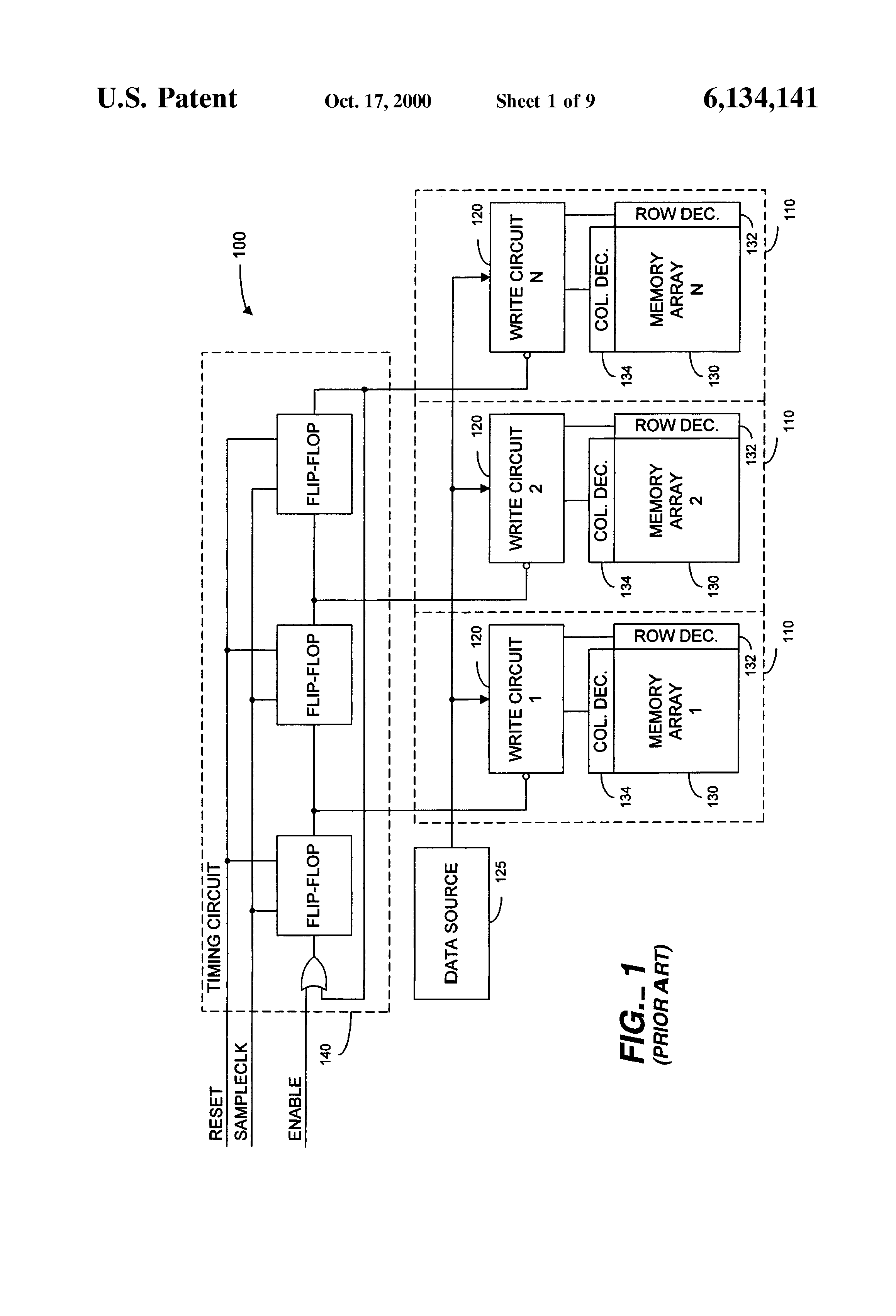
One way to increase the data bandwidth for programming is to include in an integrated circuit memory, multiple memory arrays or banks that operate in parallel or pipeline fashion. For example, U.S. Pat. No. 5,680,341, entitled "Pipelined Record and Playback for Analog Non-Volatile Memory", which is hereby incorporated by reference in its entirety, describes known analog memory systems using pipelined write operations for high data bandwidth. FIG. 1 is a block diagram of a non-volatile memory 100 including multiple write pipelines 110 for pipelined write operations. Each write pipeline 110 includes an array 130 of memory cells and a write circuit 120 that couples to a row decoder 132 and a column decoder 134 for the associated array 130. Pipelines 110 operate independently to complete separate programming operations that a timing circuit 140 sequentially starts. As a result, N pipelines 110 simultaneously perform different stages of up to N write operations for writing up to N different data values from a data source 110. The number N of pipelines 110 in memory 100 determines the maximum number of simultaneous write operations memory 100 and accordingly controls the maximum data bandwidth for writing to memory 100.

The improved data bandwidth of memory 100 comes at the cost of increased circuit complexity. In particular, each write pipeline 110 includes a separate write circuit 120. Write circuits for multi-bit-per-cell and/or analog memories and can be complex, and the redundant use of the write circuits increases required integrated circuit area and the costs of high bandwidth multi-bit-per-cell and analog/multi-level memories.

SUMMARY

In accordance with the invention, a global bias circuit in a non-volatile integrated memory circuit sequentially charges selected row lines in separate memory arrays. Each memory array preserves the charge on the selected row line during a write operation in that memory array, and the charge controls programming and/or verify voltages on the control gate of a memory cell selected for programming. Accordingly, each array does not require a latch or a sample-and-hold circuit to temporarily store a data value since the charge on the selected row line indicates the data value being written. Further, each array does not require a voltage source, resistor tree, or voltage level-shifter to provide the programming or verify voltages that depend on the value being written.

For one write operation in accordance with an embodiment of the invention, the global bias circuit charges a selected row line in a memory array to a verify voltage that is associated with a target threshold voltage to be written to a selected memory cell on the selected row line. The verify voltage Vvfy is the control gate voltage at which a sense amplifier senses a transition in the conductivity of the memory cell if the memory cell has the target threshold voltage. The write operation includes a series of program cycles and verify cycles. During the program cycles, the combination of the control gate voltage, a drain voltage, and a source voltage changes the threshold voltage of the selected memory cell. During the verify cycles, the sense amplifier senses the conductivity of the selected memory cell while the charged row line maintains the control gate of the memory cell at the verify voltage. The write operation stops when the sense amplifier senses that the memory cell is in the appropriate conductivity state during a verify cycle.

During the program cycles, a global or local control circuit and voltage source can change the voltage on the selected row line using a capacitive coupling. In particular, the control circuit, through the capacitive coupling with the selected row line, raises the row line voltage from the verify voltage to a programming voltage that depends on the initial charge on the selected row line and the capacitive coupling ratio. Since the global bias circuit selected the row line charge (or the verify voltage) according to the target threshold voltage being programmed, the programming voltage also varies according to the target threshold voltage level. A high target threshold voltage has a high verify voltage and a high programming voltage during program cycles. A low target threshold voltage has a low verify voltage and a low programming voltage during program cycles. This improves programming precision because the low programming voltage decreases the change in threshold voltage per program cycle for low target threshold voltages.

As an alternative to using a capacitive coupling to change the row line voltage during programming cycles, a column bias circuit that biases a selected column line for sensing during verify cycles provides a maximum column line bias current selected so that the programming voltage is the same as the verify voltage. Accordingly, the global bias circuit charges the selected row line to a level corresponding to both the verify voltage and the programming voltage, and the row line voltage of the selected memory cell remains constant during both program cycles and verify cycles.

One progamming process in accordance with an embodiment of the invention connects a bias circuit to charge a line that is coupled to a control gate of a memory cell to be programmed. The bias circuit is then disconnected from the line with charge from the bias circuit remaining trapped on the line. The charge on the line controls a first programming voltage that is on the control gate of the memory cell when a second programming voltage is applied to a drain of the memory cell. The combination of the first programming voltage on the control gate, the second programming voltage on the drain, and a voltage on a source of the memory cell changes a threshold voltage in the memory cell, typically by channel hot electron injection. To reach the first programming voltage the process optionally include capacitively coupling a voltage to the line to raise the line to the first programming voltage from a voltage of the bias circuit. Alternatively, the bias circuit charges the line with a voltage about equal to the first programming voltage. In either case, the programming process may include a sequence of program and verify cycles wherein the threshold voltage of the selected memory cell changes during program cycles and the verify cycles sense the threshold voltage of the selected memory cell. When a capacitive coupling is used to change the row line voltage, a maximum bias current for a column line coupled to a sense amplifier that performs the sensing is such that the capacitively coupled voltage that is required to raise the line to the first programming voltage is a supply voltage of an integrated circuit containing the memory cell. Accordingly, no charge pump is required in the control circuit that raises and lowers row line voltages.

This programming process is particularly suited to memory including multiple memory arrays because a single "global" bias circuit can be connected to for charging lines in any of the arrays. Thus, pipelined programming processes in multiple arrays can be performed using a shared global bias circuit rather than local circuitry for each array. For a multi-bit-per-cell memory, the bias circuit is a structure such as a resistor tree with multiplexing circuitry so that an input multibit data signal selects a bias voltage corresponding to the value of data signal. Thus, each charged line is charged to a voltage that is selected for the value to be written into a memory cell connected to the line.

One embodiment of the invention is a non-volatile memory such as a multi-bit-per-cell Flash memory. The memory includes a plurality of memory arrays, a bias circuit, and a control circuit. Each memory array includes memory cells arranged in rows and columns, row lines with each row line being coupled control gates of memory cells that are in a row of memory cells associated with the row line, and a row decoder coupled to the row lines. The bias circuit generates a bias signal having a voltage that depends on the value of an input data signal. The control circuit selects which of the plurality of arrays receives the bias signal from the bias circuit. During a first charging period of a write operation, the control circuit connects the bias circuit to the row decoder in a first array, and the bias circuit charges a selected row line in the first array for programming a first value in a first memory cell. During a second charging period of the write operation, the control circuit connects the bias circuit to the row decoder in a second array, and the bias circuit charges a selected row line in the second array for programming a second value in second memory cell. For a pipelined write operation, the second charging period occurs during programming of the first memory cell.

BRIEF DESCRIPTION OF THE DRAWINGS

FIG. 1 is a block diagram of a known multibank memory providing a high data bandwidth.

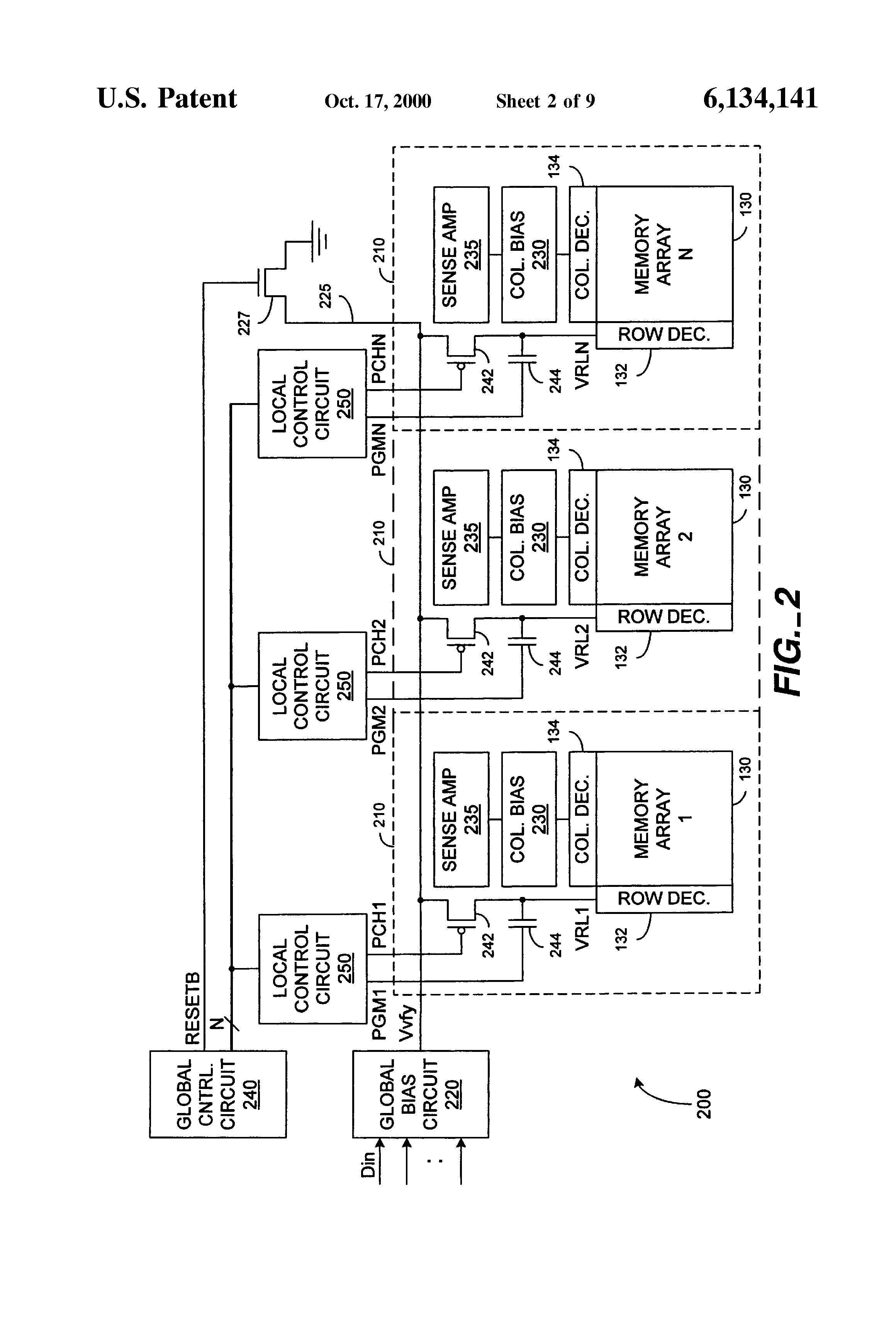
FIG. 2 is a block diagram of an embodiment of the invention where a multibank memory has a global bias circuit for charging selected row lines and a capacitive coupling for varying row line voltages during programming.

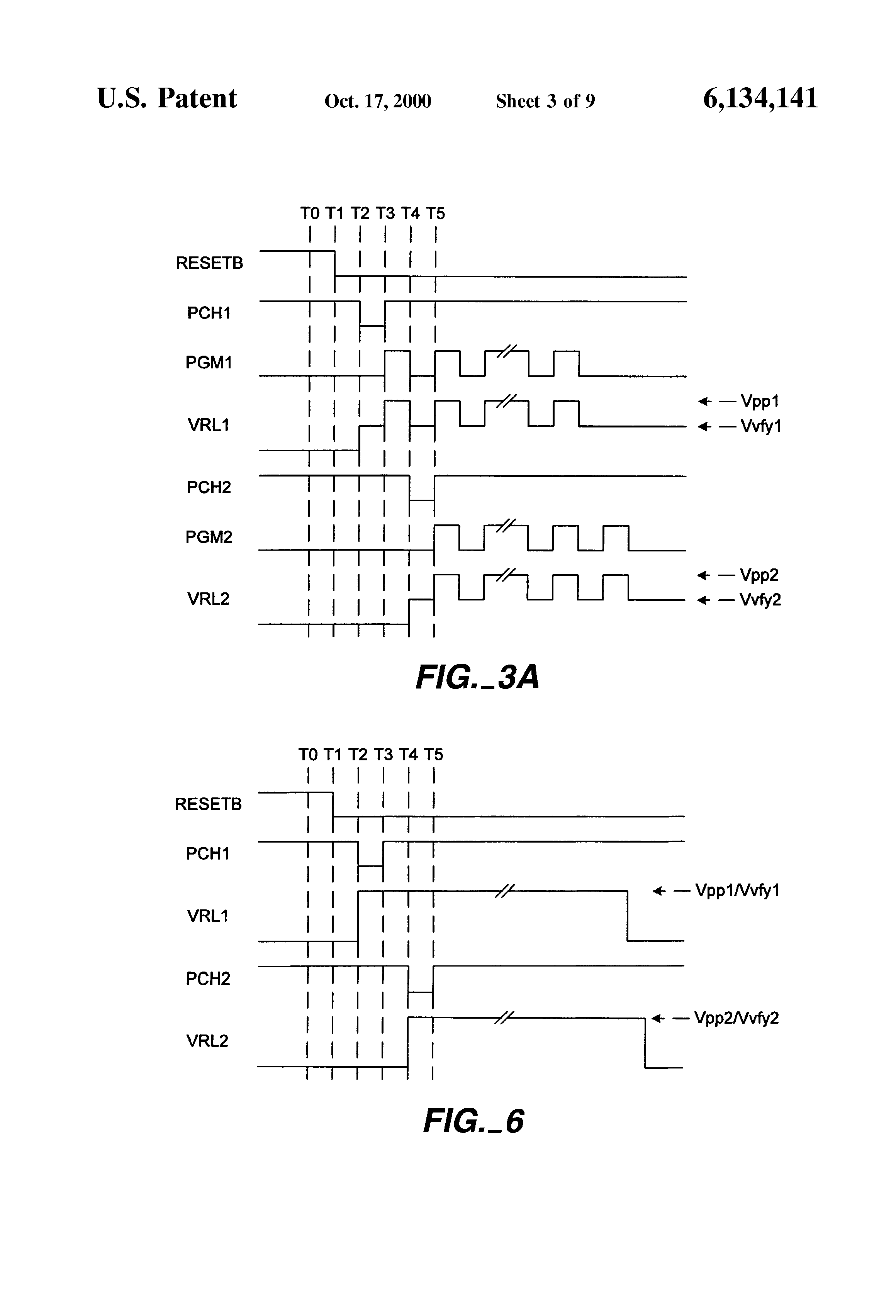
FIGS. 3A, 3B, and 3C are timing diagrams for signals generated during write operations in the memory of FIG. 2.

FIG. 4A is a schematic diagram of a sense amplifier with associated biasing circuits.

FIG. 4B shows how a column line bias current for a typical sense amplifier affects the control gate voltage that corresponds to the trip point of the sense amplifier.

FIG. 5 is a block diagram of an embodiment of the invention where a multibank memory has a global bias circuit for charging selected row lines to voltages that remain constant during write operations.

FIG. 6 is a timing diagram for a write operation in the memory of FIG. 5.

FIG. 7 is a block diagram of an embodiment of the invention having less local write control circuitry.

Use of the same reference symbols in different figures indicates similar or identical items.

DETAILED DESCRIPTION OF THE PREFERRED EMBODIMENTS

In accordance with an aspect of the invention, a dynamic write process for multi-bit-per-cell memories uses a global bias circuit to charge a selected row line for a write operation. Charge leakage from the selected row line is controlled so that the charge on the selected row line remains nearly constant during programming, but a capacitive coupling can change the voltage on the selected row line if necessary during the write operation. To avoid the need to vary the voltage on the selected row line, a bias current supplied to a column line during a sensing operation is at a level such that the row line voltage used when changing the threshold voltage of the selected memory cell is equal to a sense amplifier's trip point when the selected memory cell has the target threshold voltage.

FIG. 2 is a block diagram of a non-volatile memory 200 in accordance with an embodiment of the invention. Memory 200 includes multiple arrays 130 of Flash memory cells in respective write pipelines 210. A global control circuit 240 controls starting of write operations in write pipelines 210 of memory 200 and optionally includes a timing circuit that sequentially starts write pipelines 210 for a pipelined writing or recording of data. Such timing circuits and pipelined writing or recording operations are further described in U.S. patent application Ser. No. 09/103,623, filed Jun. 23, 1998 and U.S. patent application Ser. No. 09/128,225, filed Aug. 3, 1998 which are hereby incorporated by reference in their entirety. The pipelined writing can be used to store a data sequence that is to large to store in a signal memory cell. For example, a 32-bit value can be written to eight memory cells when each memory cell stores four bits of information, and global control circuit 240 can sequentially start eight 4-bit write operations in eight different pipelines 210.

Each memory array 130 in pipelines 210 can be a conventional non-volatile memory array that includes rows and columns of memory cells. Such memory arrays are known for storing a binary, analog, or multibit digital value in each memory cell. In arrays 130, each memory cell is, for example, a single floating gate transistor, a split gate transistor, or a multiple-transistor memory cell. In an exemplary embodiment of the invention, which is described below, memory 200 is a flash EEPROM, and each memory cell consists of a single N-channel floating gate transistor. Other memory architectures are also suitable. Control gates of the memory cells in a row of an array 130 couple to a row line associated with the row. Drains of the memory cells in a column of an array 130 couple to a column line associated with the column, and sources of the memory cells in a sector of an array 130 couple to a source line associated with the sector.

In the exemplary embodiment, each sector contains multiple columns of memory cells in an array 130, but alternative memory architectures use different kinds of sectors, for example, a sector including an entire array 130 or sectors containing one or multiple rows of memory cells. As is well known, an erase operation for Flash memory simultaneously erases all memory cells in a sector of an array. In the exemplary embodiment, where each memory cell is an N-channel floating gate transistor, an erase operation lowers the threshold voltages of all memory cells in a sector to leave memory cells in an erased state, typically having a threshold voltage less than about 2 volts.

Memory arrays 130 are separate in that a write operation in one array 130 does not directly affect write operations in other arrays 130. Each memory array 130 has local row and column lines, a local row decoder 132 coupled to the local row lines, and a local column decoder 134 coupled to the local column lines. Each row decoder 132 receives a row address signal and selects the row line coupled to a memory cell selected for a read or write operation. Each column decoder 134 similarly receives a column address signal and selects the column line coupled to the selected memory cell. In addition to the local decoders 132 and 134, global control circuit 240 includes a global decoder that decodes a global address to select which of arrays 130 performs an erase operation, a write operation, or a read operation. In one embodiment, the global decoder is such that consecutive memory addresses correspond to memory cells in different arrays. Such decoding permits separate write pipelines 210 to operate simultaneously in a pipelined fashion and provides a high bandwidth when writing a data sequence to consecutive addresses. Further, one global address may correspond to memory cells in multiple arrays 130, for example, when memory 200 has a data width (e.g., 32 bits) that greater than the width (e.g., 4 bits) of a value that can be stored in a single memory cell.

For write operations, the column decoder 134 in each array 130 connects a column line bias circuit 230 and a sense amplifier 235 to a selected column line in the array 130. Column bias circuit 230 typically includes a first pull-up device (i.e., transistor or circuit) coupled to a programming voltage Vcp and a second pull-up device coupled to a read voltage Vcr. The first pull-up device and biases the selected column line during program cycles described below, and the second pull-up device biases the selected column line during verify cycles described below. Sense amplifier 235 can be a conventional sense amplifier that senses current through a memory cell by sensing the effect the current has on a column line voltage.

In accordance with an aspect of the invention, memory 200 includes a global bias circuit 220 and a global line 225 that connects global bias circuit 220 to each write pipeline 210. Global bias circuit 220 may be, for example, a resistor tree that generates a signal Vvfy having a voltage level selected according to the value of a multibit data signal Din. The discrete voltage levels for signal Vvfy are in one-to-one correspondence with the discrete values that a memory cell can store. For example, if each memory cell in arrays 130 can store four bits of information, a 4-bit data signal Din identifies which of sixteen voltage levels global bias circuit 220 selects for signal Vvfy. Alternatively, for an analog or multi-level memory, global bias circuit 220 can be a voltage level-shifter that receives an analog or multi-level data signal and generates signal Vvfy at a level associated with the analog or multi-level value to be written in a memory cell. The case of a multi-bit-per-cell memory is described below.

At the start of a write operation, global bias circuit 220 sets signal Vvfy on global line 225 to the voltage level corresponding to a multibit value to be written in a selected write pipeline 210, and global control circuit 240 selects and activates a local control circuit 250 for a selected write pipeline 210. The activated local control circuit 250 then turns on a pull up transistor 242 that connects global line 225 to the row decoder 132 in the selected write pipeline 210, and the row decoder 132 in the selected write pipeline 210 connects a selected local row line to global line 225 via transistor 242. As a result, global bias circuit 220 charges the selected local row line and connected circuitry including a capacitor 244 to the selected voltage of signal Vvfy. Pull up transistor 242 then shuts off to disconnect the selected row line from the global line 225, and the selected row line remains charged for the write operation in the selected write pipeline 210. During that write operation, global bias circuit 220 can charge selected row lines in other arrays 130 for writing other data values.

Charge leakage from the selected row line needs to be low to hold the charge throughout a programming operation. Potential sources of leakage from a charged row line include junction leakage for transistor 242 and transistors in row decoder 132, sub-threshold conduction of transistor 242, and signal glitches that momentarily turn-on transistors that should be off. Conventional integrated circuit design techniques including circuit simulations and modeling can determine sources of leakage that must be eliminated or minimized in a particular memory architecture to limit leakage current to suitable levels.

FIG. 3A illustrates signals in memory 200 for write operations in a first and a second of the write pipelines 210. At an initial time T0, a control signal RESETB is high so that a pull down transistor 227 is on and grounds global line 225 in preparation for beginning write operations. At a time T1, global control circuit 240 deasserts control signal RESETB so that transistor 227 disconnects global line 225 from ground and allows global bias circuit 220 to charge global line 225.

At time T2, data signal Din represents a first multibit data value to be written to a selected memory cell in the first write pipeline 210. Global bias circuit 220 generates signal Vvfy at a voltage level Vvfy1 corresponding to the first data value. Global control circuit 240 asserts a signal to activate the local control circuit 250 for the first write pipeline 210, and the local control circuit 250 asserts signal PCH1 low to turn on transistor 242 in the first write pipeline 210. During the period between times T2 and T3, global bias circuit 220 charges the local row line and the capacitor 244 in the first of arrays 210 so that the signal VRL1 on the selected row line reaches voltage Vvfy1. Signal PGM1, which is on the opposite terminal of capacitor 244, grounds the opposite terminal of capacitor 244 while the selected row line charges. At time T2, local control circuit 250 deasserts signal PCH1 to turn off transistor 242 in the first of write pipelines 210. In the first of write pipelines 210, transistor 242 remains off during the remainder of the write operation. The charging period between times T1 and T2 must be sufficient to allow global bias circuit 220 to charge the selected row line to voltage Vpp1. Accordingly, the charging period depends on the current capacity of global bias circuit 220 and the capacitances of global line 225, capacitor 244, the selected row line, and other connected circuitry.

After the charging period, the write operation in write pipeline 210 includes program cycles and verify cycles. During a program cycle such as between times T3 and T4, the control gate voltage, the drain voltage, and the source voltage of the selected memory cell are at levels that cause channel hot electron injection that raises the threshold voltage of the selected memory cell. In particular, the source line coupled to the selected memory cell is grounded. A column bias circuit 230 raises the selected column line to a voltage Vcp, which is typically between about 4.5 volts and about 5.5 volts. Local control circuit 250 raises signal VRL1 to a programming voltage Vpp1 by raising signal PGM1 to voltage Vpgm.

During a verify cycle, for example, such as between times T4 and T5, a sense amplifier 235 senses the conductivity of the selected memory cell while the control gate signal VRL1 of the selected memory cell is at voltage Vvfy1. Local control circuit 250 lowers the control gate voltage VRL1 back to Vvfy1 by grounding signal PGM1. If the selected memory cell stops conducting sufficient current, sense amplifier 2325 trips indicating the threshold voltage of the selected memory cell has risen to the level voltage Vvfy1 indicates. The write operation is then complete. For an accurate write operation, global bias circuit 220 during the charging period must generate signal Vvfy at a voltage that corresponds to the trip point of the sense amplifier 235 when the selected memory cell has a threshold voltage in the interval corresponding to the data value being written.

Another aspect of memory 200 is that global control circuit 240 can start a write operation in another write pipeline 210 while the first write pipeline 210 executes a write operation. In FIG. 3A, control circuit 240 starts the second write pipeline 210 on a write operation at time T4. In particular, data signal Din represents a second data value at time T4, and global bias circuit 220 generates signal Vvfy at a voltage Vvfy2 that corresponds to the second data value. At time T4, global control circuit 240 activates the local control circuit 250 for the second write pipeline 210, and during the interval between times T4 and T5, local control circuit 250 asserts signal PCH2 low to turn on transistor 242 in the second write pipeline 210. Global bias circuit 220 charges global line 225 and the selected local row line in the second write pipeline 210 to voltage Vvfy2. The write operation in second write pipeline is same as the write operation in the first write pipeline. Signal PGM2 rises to voltage Vpgm and raises row line signal VRL2 to voltage Vpp2 during program cycles. Signal PGM2 is grounded during verify cycles so that signal VRL2 is at voltage Vvfy2. Column bias circuit 230 controls the column line voltage to cause channel hot electron injection during program cycles, and sense amplifier 235 senses whether the selected memory cell has the threshold voltage corresponding to voltage Vvf2.

In memory 200, write pipelines 210 have independent signals PGM1 to PGMN, and each of signals PGM1 to PGMN stops pulsing at the end of a write operation in the associate write pipeline 210. Additionally or alternatively, column bias circuit 230 can change the column line and/or source line voltages to stop channel hot electron injection even when the associated one of signals PGM1 to PGMN is high. In yet another alternative embodiment, all pipelines 210 use the same signal PGM which continues to pulse, and column bias circuits 230 stop channel hot electron injection when a memory cell in the associated array reaches the target threshold voltage.

Equation 1 indicates how a programming voltage Vpp depends on the charge on the selected row line, the voltage Vpgm of signal PGM, and capacitive coupling ratio C of signal PGM to the selected row line.

For a typical Flash memory cell, voltage Vpp needs to be in a range between about 7 volts and about 10 volts to achieve a typical threshold voltage window of about 3 volts. According to Equation 1, the programming voltage Vpp depends linearly on the voltage of signal Vvfy in the write pipeline. When the target threshold voltage for a memory cell is high, signals Vvfy and Vpp have correspondingly high voltages, and the programming voltage Vpp causes a relatively large change in threshold voltage during each program cycle. When the target threshold voltage for a memory cell is low, signals Vvfy and Vpp have correspondingly low voltages, and the programming voltage Vpp causes a relatively small change in threshold voltage during each program cycle. Accordingly, about the same number of program cycles are required to reach the target threshold voltage regardless of whether the target threshold voltage is high or low, and the resolution for writing threshold voltages is uniform across the range of target threshold voltages.

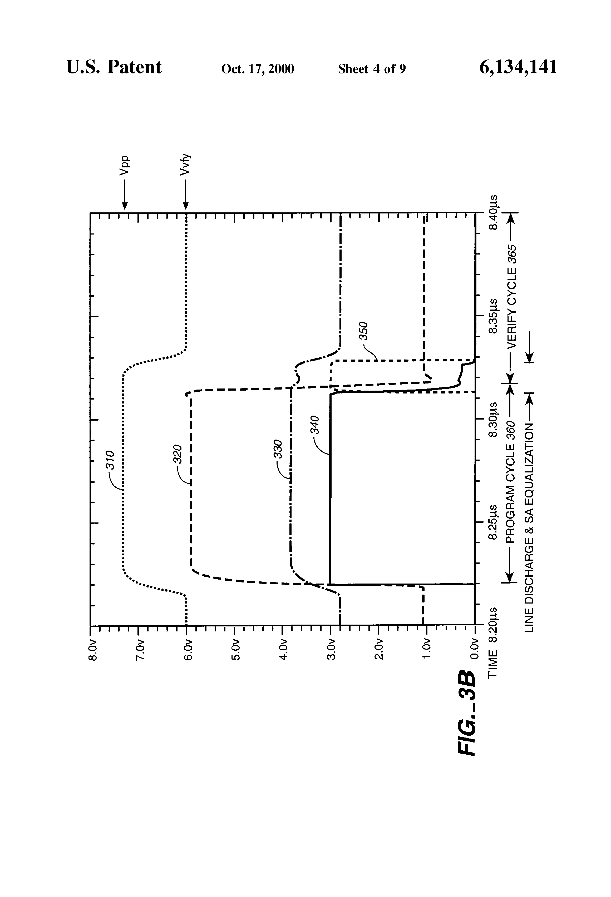
FIGS. 3B and 3C show more detailed plots of signals during program cycles 360 and 370 and verify cycles 365 and 375 in the exemplary embodiment of the invention. In FIGS. 3B and 3C, plots 310, 320, 330, 340, and 350 respectively represents the signal VRL on the selected row line, the signal on the selected column line, the voltage of the floating gate in the selected memory cell, an output signal SAOUT from a sense amplifier coupled to the selected column line, and an equalization signal EQ to prepare the selected column line for sensing. At the start of program cycle 360, the capacitive coupling of signal PGM to selected row line raises signal VRL on the selected row line from the verify voltage Vvfy (about 6V in this example) to the programming voltage Vpp (about 7.2 volts in this example).

At about the same time that signal VRL rises to the programming voltage Vpp, column bias circuit 230 raises the voltage on the selected column line to a programming voltage Vcp of about 6 volts. (The source of the selected memory cell remains grounded.) The voltage on the floating gate of the selected memory cell rises in response to the programming voltages Vpp and Vcp, but injection current charges the floating gate to slowly lower the floating gate voltage and increase the threshold voltage of the selected memory cell during program cycle 360. In the example of FIG. 3B, the program cycle is about 100 ns. At the end of program cycle 360, column bias circuit 230 drops the voltage on the selected column line to a verify voltage Vcr which is less than about 1.5 to 2.0 volts in preparation for verify cycle 365.

In verify cycle 365, the selected memory cell conducts sufficient current to indicate that the selected memory cell's threshold voltage has not risen to the target threshold voltage level. For the verify cycle, the control gate voltage signal 310 is initially left high so that the memory cell conducts while column bias circuit 230 lowers the column line voltage to Vcr. The output signal SAOUT of sense amplifier 235 falls because the selected memory cell conducts sufficient current for sense amplifier 235 to sense while the control gate is at programming voltage Vpp. During this time, equalization signal 350 is asserted to prepare sense amplifier 235 for sensing. When local control circuit 250 lowers signal VRL 310 to Vvfy, the equalization signal is deasserted, and sense amplifier 235 senses for current through the selected memory cell. During verify cycle 365, the threshold voltage of the selected memory cell is below the target threshold voltage. Sense amplifier 235 senses that current through the selected memory cell is about equal or greater than the current from column bias circuit 230, and the output signal 340 from sense amplifier 235 remains low.

FIG. 3C shows a program cycle 370 during which the threshold voltage of the selected memory cell rises to the target threshold voltage. Program cycle 370 is otherwise the same as program cycle 360 described above. During the following verify cycle 375, sense amplifier 235 senses that the current through the selected memory cell is less than the maximum current from column bias circuit 230, and the output signal 340 rises (at time 8.58 μs) when sense amplifier 235 trips.

FIG. 4A illustrates a sense amplifier with circuitry for biasing the column line coupled to a selected memory cell. Such circuitry is suitable for use in memory 200 of FIG. 2. In FIG. 4, the bias circuitry includes a current mirror 410 having a reference current path through a reference column line of an associated array. Current mirror 410 also includes a normal current path and a high current path coupled to the selected column line through a local column decoder. A transistor 412 in the reference current path has its gate and drain coupled to the gates of transistors 414 and 416 in the normal and high current paths respectively. Signals NORMAL and HIGH selected which of the normal and high current paths supply the bias current to the selected column line for sensing. Transistor 416 has X times the channel width of transistor 414, and when the high current path is selected, mirror circuit 410 supplies a maximum bias current that is X times the maximum current that the normal current path supplies.

A pair of inverters 420 and 430 connect in series to a node 440 between current mirror 410 and the selected column line. For sensing, equalization signal EQ is asserted and a transistor 425 equalize the voltages on the input and output terminals of inverter 420 and puts inverter 420 in an unstable state to provide quicker sensing. When signal EQ is deasserted, the states of inverter 420 and inverter 430 change according to the voltage on node 440. A circuit 450 amplifies voltage swings that the selected column line causes on node 440 by drawing a current through the selected memory cell. At the trip point of the sense amplifier, the selected column line draws a current that is equal to the bias current from current mirror 410. Accordingly, the trip point of the sense amplifier changes according to the sizes of transistors 414 and 416, which are chosen during circuit design, and according to signals NORMAL and HIGH, which can be dynamically chosen during memory operation.

In FIG. 2, when the maximum current from column bias circuit 230 is very low during a verify cycle, the sense amplifier can sense a small current through the selected memory cell because even a small current through the selected memory cell pulls down the column line voltage. In this case, voltage Vvfy, which is the control gate voltage of the selected memory cell when sense amplifier 235 trips, is approximately equal to the target threshold voltage for the selected memory cell, and the range of signal Vvfy is about the same as the useable range of threshold voltages for memory cells, e.g., between about 3 volts and about 6 volts for typical flash memory cells. Since the suitable range for programming voltage Vpp on the control gate is typically between 7 and 10 volts and a maximum reasonably achievable capacitive coupling to the selected column line is about 70%, voltage Vpgm needs to be more than 5 volts to raise voltage Vpp into the desired range. Accordingly, a charge pump or other high voltage source is needed to raise a typical supply voltage Vcc of about 3 or 5 volts to the required voltage for Vpgm.

In accordance with another aspect of the invention, column bias circuit 230 provides a high bias current on the selected column line to raise the control gate voltage corresponding to the trip point of sense amplifier 235. FIG. 4B illustrates the effect of column line bias current on the control gate voltage corresponding to the trip point of a typical sense amplifier. For a plot 480 in FIG. 4B, a bias circuit supplies a maximum current of about 1 μA to the selected column line, and when a memory cell has a floating gate charged to between about -0.5 volts and -1 volt, a control gate voltage between 2 volts and 3 volts causes the memory cell to conduct a current sufficient to trip the sense amplifier. The control gate voltage must be above about 6 volts to trip the sense amplifier when the floating gate voltage is less than -3 volts and the column line bias current is about 1 μA

If column line bias current is larger, the control gate voltage corresponding to the sense amplifier's trip point for a particular memory cell is higher because the memory cell must conduct a larger current in order to pull the column line voltage low enough to trip the sense amplifier. For plot 490, the bias current is 100 μA, and a control gate voltage of about 7 volts causes the memory cell to conduct a current sufficient to trip the sense amplifier when a memory cell has a floating gate charged to about -1 volt which provides a threshold voltage of about 2.5 volts. With the column line bias current at about 100 μA, the control gate voltage must be above about 10 volts to trip the sense amplifier when the floating gate voltage is less than -3 volts which provides a threshold voltage of about 6 volts. Accordingly, raising the column line bias current requires increasing the voltage of signal Vvfy for each data value. However, a higher voltage for signal Vvfy means that voltage Vpgm can be lower and still achieve a programming voltage Vpp in the required range. In one embodiment of memory 200 of FIG. 2, column bias circuit 230 selects the column line bias current for sense amplifier 235 during verify cycles so that voltage Vpgm is equal to the supply voltage Vcc. In this embodiment, local control circuits 250 do not require a charge pump to generate voltage Vpgm.

Signal Vvfy must be accurately set according to the bias current that the sense amplifier 235 uses during verify cycles. A read operation can use the same sense amplifier 235 and bias circuit 230. For example, one read operation sweeps a selected row line voltage across a voltage range. The voltage on the row line when sense amplifier trips indicates the stored value in the memory cell and can be converted to a multibit value. U.S. Pat. Nos. 5,748,533 and 5,748,534, both issued May 5, 1998, describe other suitable read methods using sense amplifiers to determine threshold voltages and are hereby incorporated by reference in their entirety. During a read, the high column line bias current used during verify operations results in high row line voltages when the sense amplifier trips. Alternatively, to lower the row line voltage, sense amplifier 235 can use a column line bias current during read operations that is lower than the bias current used during verify cycles.

In accordance with yet a further aspect of the invention, the column line bias current can be raised until the required voltages Vvfy for verify cycles are in the range suitable for program cycles. In this case, the control line voltage for the selected memory cell does not need to be raised for program cycles. As illustrated in FIG. 5, a memory 500 can thus eliminate the capacitive coupling to the selected row line and local control circuitry that generates signals PCM1 to PCMN. A simpler global control circuit 540 can control transistors 242 to turn on the appropriate transistors 242 during the charging periods for write pipelines 510.

FIG. 6 shows timing diagrams for signals in memory 500 during write operations in the first and second write pipelines 210. In FIG. 6, signal PCH1 turns on transistor 242 in the first write pipeline 210 during a charging period from T2 to T3, and global bias circuit 220 charges the selected row line to voltage Vvfy1 (which is equal to Vpp1 ) until the end of the write operation in the first write pipeline 210. During the write operation in the first write pipeline, row line voltage VRL1 remains nearly constant at a voltage Vvfy1, and column bias circuit 230 alternates the drain voltage between programming voltage Vcp for program cycles and voltage Vcr for verify cycles. Similarly, signal PCH2 turns on transistor 242 in the second write pipeline 210 during a charging period from T4 to T5, and row line voltage VRL2 remains nearly constant at voltage Vvfy2 (which is equal to Vpp2) during program and verify cycles in the second write pipeline 210.

As illustrated in FIG. 7, a global control circuit 740 in a memory 700 can generate the same signal PGM which all write pipelines 210 use to change the row line voltages for program cycles and verify cycles. An optional transistor (not shown) between capacitor 244 and control circuit 240 can stop pulsing of the row line voltage after the write operation reaches the target threshold voltage. Alternatively, column bias circuit 230 changes the biasing of the selected column line to prevent channel hot electron injection after the threshold voltage of the selected memory cell reaches the target threshold voltage.

Although the invention has been described with reference to particular embodiments, the description is only an example of the invention's application and should not be taken as a limitation. Various adaptations and combinations of features of the embodiments disclosed are within the scope of the invention as defined by the following claims.
Claims (17)

  1. A method for programming a memory cell, comprising: connecting a bias circuit to charge a line that is coupled to a control gate of the memory cell; disconnecting the bias circuit from the line, wherein charge remains trapped on the line and controls a first programming voltage on the control gate of the memory cell; and applying a second programming voltage to a drain of the memory cell, wherein a combination of the first programming voltage on the control gate, the second programming voltage on the drain, and a voltage on a source of the memory cell changes a threshold voltage in the memory cell.
  2. The method of claim 1, wherein the bias circuit charges the line to a first voltage, and the method further comprises capacitively coupling a second voltage to the line to raise the line from the first voltage to the first programming voltage.
  3. The method of claim 2, wherein the first voltage is a voltage at which a sense amplifier coupled to the line sense a change in conductivity of the memory cell when the memory cell has a target threshold voltage, the method further comprising: (a) capacitively coupling the second voltage to raise the line from the first voltage to the first programming voltage for a program cycle during which the threshold voltage in the memory cell changes; (b) removing the second voltage from the capacitive coupling so that the line falls from the first programming voltage to the first voltage during a verify cycle; (c) sensing the conductivity of the memory cell during the verify cycle; and (d) repeating steps (a), (b) and (c) until sensing determines that the threshold voltage of the memory cell has reached the target threshold voltage.
  4. The method of claim 3, further comprising selecting a maximum bias current for a column line coupled to a sense amplifier that performs the sensing, wherein the maximum bias current selected is such that second voltage, which is required to raise the line from the first voltage to the first programming voltage, is a supply voltage of an integrated circuit containing the memory cell.
  5. The method of claim 1, wherein connecting the bias circuit to the line charges the line to the first programming voltage.
  6. The method of claim 5, further comprising: (a) applying the second programming voltage to the drain during a program cycle during which the threshold voltage in the memory cell changes; (b) applying a second voltage to the drain during a verify cycle, wherein the control gate remains at a constant voltage through the program cycle and the verify cycle; (c) sensing the conductivity of the memory cell during the verify cycle; and (d) repeating steps (a), (b) and (c) until sensing determines that the threshold voltage of the memory cell has reached a target threshold voltage.
  7. The method of claim 6, further comprising selecting a maximum bias current for a column line coupled to a sense amplifier that performs the sensing, wherein the maximum bias current selected is such that the first programming voltage corresponds to a trip point of the sense amplifier.
  8. The method of claim 1, wherein the combination of the first programming voltage on the control gate, the second programming voltage on the drain, and the voltage on the source of the memory cell causes channel hot electron injection into a floating gate in the memory cell.
  9. The method of claim 1, wherein the memory cell is in a first array from among a plurality of memory arrays in a non-volatile memory, and the line is a first row line coupled to control gates of a row of memory cells in the first array.
  10. The method of claim 1, wherein connecting the bias circuit comprises: applying a data signal to the bias circuit, the data signal indicating a value to be written in the memory cell; generating from the bias circuit a first voltage that is selected according the value to be written; and charging the line to the first voltage.
  11. The method of claim 10, wherein the value is a multibit digital value.
  12. A method for programming a memory cell, comprising: connecting a bias circuit to charge a line that is coupled to a control gate of the memory cell, wherein the memory cell is in a first array from among a plurality of memory arrays in a non-volatile memory, and the line is a first row coupled to control gates of a row of memory cells in the first array; disconnecting the bias circuit from the line, wherein charge remains trapped on the line and controls a first programming voltage on the control gate of the memory cell; and applying a second programming voltage to a drain of the memory cell, wherein a combination of the first programming voltage on the control gate, the second programming voltage on the drain, and a voltage on a source of the memory cell changes a threshold voltage in the memory cell; connecting the bias circuit to charge a second row line in a second array from among the plurality of memory arrays, the second row line being coupled to a control gate of a second memory cell in the second array; using the bias circuit to charge the second row line for programming operation to be performed on the second memory cell; and performing the programming operation on the second memory cell while also programming the memory cell in the first array.
  13. The method of claim 12, wherein the programming operation on the second memory cell comprises: disconnecting the bias circuit from the second row line, wherein charge remains trapped on the second row line and controls a third programming voltage on the control gate of the second memory cell; and applying the second programming voltage to a drain of the second memory cell, wherein a combination of the third programming voltage on the control gate of the second memory cell, the second programming voltage on the drain of the second memory cell, and a voltage on a source of the second memory cell changes a threshold voltage in the second memory cell.
  14. The method of claim 13, further comprising: applying a data signal to the bias circuit generating from the bias circuit a first voltage that is selected according a first value of the date signal, the first value being a data value to be written to the memory cell in the first array, wherein the bias circuit applies the first voltage to the first row line, the first voltage controlling the charge trapped on the first row line and thereby controlling the first programming voltage; and generating from the bias circuit a second voltage that is selected according a second value of the date signal, the second value being a date value to be written to the second memory cell, wherein the bias circuit applies the second voltage to the second row line, the second voltage controlling the charge trapped on the second row line and thereby controlling the third programming voltage.
  15. The method of claim 14, wherein the first value and the second value are multibit digital values.
  16. A non-volatile memory comprising: a plurality of memory arrays, each memory array including memory cells arranged in rows and columns, row lines with each row line being coupled control gates of memory cells that are in a row of memory cells associated with the row line, and a row decoder coupled to the row lines; a bias circuit having a input port for a date signal, the bias circuit generating a bias signal having a voltage that depends on a value of the date signal; and a control circuit coupled to the bias circuit and the plurality of memory arrays, the control circuit selecting which of the plurality of arrays receives the bias signal from the bias circuit, wherein: during a first charging period of a write operation, the control circuit connects the bias circuit to the row decoder in a first array from among the plurality of arrays, and the bias circuit charges a selected row line in the first array for programming a first memory cell which is in the first array; during a second charging period of the write operation, the control circuit connects the bias circuit to the row decoder in a second array from among the plurality of arrays, and the bias circuit charges a selected row line in the second array for programming a second memory cell which is in the second array; and the second charging period occurs during programming of the first memory cell.
  17. The memory of claim 16, wherein the memory is a multi-bit-per-cell memory.

Publications

Related applications (3)

  1. US09/224,656

    Priority application

  2. US09/224,656

    Claims priority

  3. US09/224,656

    Patent family

Record timeline

  1. Application filed by SanDisk Corp

  2. Priority to US09/224,656

  3. Assigned to INVOX TECHNOLOGY

  4. Application granted

  5. Publication of US6134141A

  6. Assigned to SANDISK CORPORATION

  7. Assigned to SANDISK TECHNOLOGIES INC.

  8. Assigned to SANDISK TECHNOLOGIES LLC

  9. Anticipated expiration

  10. Expired - LifetimeCurrent

Legal events

  1. AS

    Assignment

    Owner name: INVOX TECHNOLOGY, CALIFORNIA

    Free format text: ASSIGNMENT OF ASSIGNORS INTEREST;ASSIGNOR:WONG, SAU-CHING;REEL/FRAME:009820/0816

    Effective date: 19990303

  2. STCF

    Information on status: patent grant

    Free format text: PATENTED CASE

  3. AS

    Assignment

    Owner name: SANDISK CORPORATION, CALIFORNIA

    Free format text: ASSIGNMENT OF ASSIGNORS INTEREST;ASSIGNOR:INVOX TECHNOLOGY;REEL/FRAME:011812/0888

    Effective date: 19990920

  4. FPAY

    Fee payment

    Year of fee payment: 4

  5. FPAY

    Fee payment

    Year of fee payment: 8

  6. AS

    Assignment

    Owner name: SANDISK TECHNOLOGIES INC., TEXAS

    Free format text: ASSIGNMENT OF ASSIGNORS INTEREST;ASSIGNOR:SANDISK CORPORATION;REEL/FRAME:026224/0761

    Effective date: 20110404

  7. FPAY

    Fee payment

    Year of fee payment: 12

  8. AS

    Assignment

    Owner name: SANDISK TECHNOLOGIES LLC, TEXAS

    Free format text: CHANGE OF NAME;ASSIGNOR:SANDISK TECHNOLOGIES INC;REEL/FRAME:038813/0004

    Effective date: 20160516

Patent citations (2)

  1. US5784315A

    Semiconductor memory device

    Kabushiki Kaisha Toshiba · July 21, 1998 · Examiner cited

  2. US5587951A

    High speed, low voltage non-volatile memory

    Atmel Corporation · December 24, 1996 · Examiner cited

Cited by (140)

  1. US20050248986A1

    High data rate write process for non-volatile flash memories

    Wong Sau C · November 10, 2005 · Examiner cited

  2. US7349255B2

    High data rate write process for non-volatile flash memories

    Sandisk Corporation · March 25, 2008 · Examiner cited

  3. US6327186B1

    Non-volatile semiconductor memory including memory cells having different charge exchange capability

    Fujitsu Limited · December 4, 2001 · Examiner cited

  4. US6330185B1

    High bandwidth multi-level flash memory using dummy memory accesses to improve precision when writing or reading a data stream

    Multi Level Memory Technology · December 11, 2001

  5. US6278633B1

    High bandwidth flash memory that selects programming parameters according to measurements of previous programming operations

    Multi Level Memory Technology · August 21, 2001

  6. US6532556B1

    Data management for multi-bit-per-cell memories

    Multi Level Memory Technology · March 11, 2003

  7. US6259627B1

    Read and write operations using constant row line voltage and variable column line load

    Multi Level Memory Technology · July 10, 2001

  8. US6363008B1

    Multi-bit-cell non-volatile memory with maximized data capacity

    Multi Level Memory Technology · March 26, 2002

  9. US6558967B1

    Multi-bit-per-cell memory system with numbers of bits per cell set by testing of memory units

    Multi Level Memory Technology · May 6, 2003

  10. US6754128B2

    Non-volatile memory operations that change a mapping between physical and logical addresses when restoring data

    Multi Level Memory Technology · June 22, 2004

  11. US6396744B1

    Flash memory with dynamic refresh

    Multi Level Memory Technology · May 28, 2002

  12. US7079422B1

    Periodic refresh operations for non-volatile multiple-bit-per-cell memory

    Samsung Electronics Co., Ltd. · July 18, 2006

  13. US6522586B2

    Dynamic refresh that changes the physical storage locations of data in flash memory

    Multi Level Memory Technology · February 18, 2003

  14. US6856568B1

    Refresh operations that change address mappings in a non-volatile memory

    Multi Level Memory Technology · February 15, 2005

  15. US6301151B1

    Adaptive programming method and apparatus for flash memory analog storage

    Information Storage Devices, Inc. · October 9, 2001 · Examiner cited

  16. US6466476B1

    Data coding for multi-bit-per-cell memories having variable numbers of bits per memory cell

    Multi Level Memory Technology · October 15, 2002

  17. US8004912B2

    Block redundancy implementation in hierarchical rams

    Broadcom Corporation · August 23, 2011

  18. US6646954B2

    Synchronous controlled, self-timed local SRAM block

    Broadcom Corporation · November 11, 2003 · Examiner cited

  19. US20040105338A1

    Synchronous controlled, self-timed local SRAM block

    Winograd Gil I. · June 3, 2004 · Examiner cited

  20. US20040085804A1

    Synchronous controlled, self-timed local SRAM block

    Winograd Gil I. · May 6, 2004 · Examiner cited

  21. US7154810B2

    Synchronous controlled, self-timed local SRAM block

    Broadcom Corporation · December 26, 2006

  22. US6947350B2

    Synchronous controlled, self-timed local SRAM block

    Broadcom Corporation · September 20, 2005

  23. US20050128854A1

    Synchronous controlled, self-timed local SRAM block

    Winograd Gil I. · June 16, 2005 · Examiner cited

  24. US20090316512A1

    Block redundancy implementation in heirarchical ram's

    Esin Terzioglu · December 24, 2009 · Examiner cited

  25. US6882591B2

    Synchronous controlled, self-timed local SRAM block

    Broadcom Corporation · April 19, 2005

  26. US6490218B1

    Digital memory method and system for storing multiple bit digital data

    Matrix Semiconductor, Inc. · December 3, 2002 · Examiner cited

  27. US7215580B2

    Non-volatile memory control

    Lexar Media, Inc. · May 8, 2007 · Examiner cited

  28. US20050018527A1

    Non-volatile memory control

    Gorobets Sergey Anatolievich · January 27, 2005 · Examiner cited

  29. US7000063B2

    Write-many memory device and method for limiting a number of writes to the write-many memory device

    Matrix Semiconductor, Inc. · February 14, 2006

  30. US6813194B2

    Bias distribution network for digital multilevel nonvolatile flash memory

    Silicon Storage Technology, Inc. · November 2, 2004 · Examiner cited

  31. US20030128594A1

    Bias distribution network for digital multilevel nonvolatile flash memory

    Tran Hieu Van · July 10, 2003 · Examiner cited

  32. US6898145B2

    Distributed, highly configurable modular predecoding

    Broadcom Corporation · May 24, 2005

  33. US6760243B2

    Distributed, highly configurable modular predecoding

    Broadcom Corporation · July 6, 2004 · Examiner cited

  34. US20040208037A1

    Distributed, highly configurable modular predecoding

    Winograd Gil I. · October 21, 2004 · Examiner cited

  35. US7453736B2

    Methods of erasing and designing electrically erasable charge trap nonvolatile memory cells having erase threshold voltage that is higher than an initial threshold voltage

    Samsung Electronics Co., Ltd. · November 18, 2008

  36. US20050237783A1

    Electrically erasable charge trap nonvolatile memory cells having erase threshold voltage that is higher than an initial threshold voltage

    Samsung Electronics Co., Ltd. · October 27, 2005 · Examiner cited

  37. US6947330B2

    Electrically erasable charge trap nonvolatile memory cells having erase threshold voltage that is higher than an initial threshold voltage

    Samsung Electronics Co., Ltd. · September 20, 2005 · Examiner cited

  38. US7170795B2

    Electrically erasable charge trap nonvolatile memory cells having erase threshold voltage that is higher than an initial threshold voltage

    Samsung Electronics Co., Ltd. · January 30, 2007

  39. US20070103990A1

    Methods of erasing and designing electrically erasable charge trap nonvolatile memory cells having erase threshold voltage that is higher than an initial threshold voltage

    Samsung Electronics Co., Ltd. · May 10, 2007 · Examiner cited

  40. US20030210573A1

    Electrically erasable charge trap nonvolatile memory cells having erase threshold voltage that is higher than an initial threshold voltage, and methods of erasing and designing same

    Chang-Hyun Lee · November 13, 2003 · Examiner cited

  41. US6567304B1

    Memory device and method for reliably reading multi-bit data from a write-many memory cell

    Matrix Semiconductor, Inc · May 20, 2003

  42. EP1418592A1

    Semiconductor memory device and control method thereof

    Sharp Kabushiki Kaisha · May 12, 2004 · Examiner cited

  43. CN100446121C

    Semiconductor memory device and manufacturing method thereof

    夏普株式会社 · December 24, 2008 · Examiner cited

  44. US6862213B2

    Semiconductor memory device and control method thereof

    Sharp Kabushiki Kaisha · March 1, 2005

  45. US20040130938A1

    Semiconductor memory device and control method thereof

    Sharp Kabushiki Kaisha · July 8, 2004 · Examiner cited

  46. US7630237B2

    System and method for programming cells in non-volatile integrated memory devices

    Sandisk Corporation · December 8, 2009

  47. US20060291285A1

    System and method for programming cells in non-volatile integrated memory devices

    Nima Mokhlesi · December 28, 2006 · Examiner cited

  48. US7046551B2

    Nonvolatile memories with asymmetric transistors, nonvolatile memories with high voltage lines extending in the column direction, and nonvolatile memories with decoding circuits sharing a common area

    Mosel Vitelic, Inc. · May 16, 2006

  49. US20040190343A1

    Nonvolatile memories with asymmetric transistors, nonvolatile memories with high voltage lines extending in the column direction, and nonvolatile memories with decoding circuits sharing a common area

    Jongmin Park · September 30, 2004 · Examiner cited

  50. US20050041475A1

    Program voltage generation circuit for stably programming flash memory cell and method of programming flash memory cell

    Samsung Electronics Co., Ltd. · February 24, 2005 · Examiner cited

  51. US6865110B1

    Program voltage generation circuit for stably programming flash memory cell and method of programming flash memory cell

    Samsung Electronics Co., Ltd. · March 8, 2005 · Examiner cited

  52. US20050162913A1

    Method of reading NAND memory to compensate for coupling between storage elements

    Jian Chen · July 28, 2005 · Examiner cited

  53. US20080180998A1

    Method of reading nand memory to compensate for coupling between storage elements

    Jian Chen · July 31, 2008 · Examiner cited

  54. US7372730B2

    Method of reading NAND memory to compensate for coupling between storage elements

    Sandisk Corporation · May 13, 2008

  55. US7149119B2

    System and method of controlling a three-dimensional memory

    Matrix Semiconductor, Inc. · December 12, 2006

  56. US20060067127A1

    Method of programming a monolithic three-dimensional memory

    Matrix Semiconductor, Inc. · March 30, 2006 · Examiner cited

  57. US10978159B2

    Programming nonvolatile memory cells through a series of predetermined threshold voltages

    Samsung Electronics Co., Ltd. · April 13, 2021

  58. US9449682B2

    Reading a multi-bit value from a memory cell

    Sau Ching Wong · September 20, 2016

  59. US9576647B2

    Parallel programming of nonvolatile memory cells

    Sau Ching Wong · February 21, 2017

  60. US10468108B2

    Programming nonvolatile memory cells using resolution-based and level-based voltage increments

    Samsung Electronics Co., Ltd. · November 5, 2019

  61. US11200954B2

    Programming nonvolatile memory cells through a series of predetermined threshold voltages

    Samsung Electronics Co., Ltd. · December 14, 2021

  62. US10468107B2

    Programming nonvolatile memory cells through a series of predetermined threshold voltages

    Samsung Electronics Co., Ltd. · November 5, 2019

  63. US10535407B2

    Adaptive parallel writing to nonvolatile memory cells

    Samsung Electronics Co., Ltd. · January 14, 2020

  64. US11114164B2

    Programming nonvolatile memory cells through a series of predetermined threshold voltages

    Samsung Electronics Co., Ltd. · September 7, 2021

  65. US7656710B1

    Adaptive operations for nonvolatile memories

    Sau Ching Wong · February 2, 2010

  66. US8014197B2

    System and method for programming cells in non-volatile integrated memory devices

    Sandisk Technologies Inc. · September 6, 2011

  67. US20100039859A1

    System and Method for Programming Cells in Non-Volatile Integrated Memory Devices

    Nima Mokhlesi · February 18, 2010 · Examiner cited

  68. US7349264B2

    Alternate sensing techniques for non-volatile memories

    Sandisk Corporation · March 25, 2008

  69. US7460406B2

    Alternate sensing techniques for non-volatile memories

    Sandisk Corporation · December 2, 2008

  70. US7616481B2

    Memories with alternate sensing techniques

    Sandisk Corporation · November 10, 2009

  71. US20080123414A1

    Alternate Sensing Techniques for Non-Volatile Memories

    Nima Mokhlesi · May 29, 2008 · Examiner cited

  72. US20070171744A1

    Memories with alternate sensing techniques

    Nima Mokhlesi · July 26, 2007 · Examiner cited

  73. US20070147113A1

    Alternate sensing techniques for non-volatile memories

    Nima Mokhlesi · June 28, 2007 · Examiner cited

  74. US20110170348A1

    Analog interface for a flash memory die

    Apple Inc. · July 14, 2011 · Examiner cited

  75. US8000134B2

    Off-die charge pump that supplies multiple flash devices

    Apple Inc. · August 16, 2011

  76. US20090323418A1

    Use of Alternative Value in Cell Detection

    Cornwell Michael J · December 31, 2009 · Examiner cited

  77. US7639542B2

    Maintenance operations for multi-level data storage cells

    Apple Inc. · December 29, 2009

  78. US20100070801A1

    Maintenance operations for multi-level data storage cells

    Apple Inc. · March 18, 2010 · Examiner cited

  79. US20100070798A1

    Maintenance Operations for Multi-Level Data Storage Cells

    Apple Inc. · March 18, 2010 · Examiner cited

  80. US20100070799A1

    Dynamic cell bit resolution

    Apple Inc. · March 18, 2010 · Examiner cited

  81. US7701797B2

    Two levels of voltage regulation supplied for logic and data programming voltage of a memory device

    Apple Inc. · April 20, 2010

  82. US20100157674A1

    Two Levels of Voltage Regulation Supplied for Logic and Data Programming Voltage of a Memory Device

    Apple Inc. · June 24, 2010 · Examiner cited

  83. US7773022B2

    Operating NAND cells using multiple levels for each data value

    Apple Inc. · August 10, 2010

  84. US20070263469A1

    Two Levels of Voltage Regulation Supplied for Logic and Data Programming Voltage of a Memory Device

    Apple Inc. · November 15, 2007 · Examiner cited

  85. US7852690B2

    Multi-chip package for a flash memory

    Apple Inc. · December 14, 2010

  86. US7852674B2

    Dynamic cell bit resolution

    Apple Inc. · December 14, 2010

  87. US7859908B2

    Iterative memory cell charging based on reference cell value

    Apple Inc. · December 28, 2010

  88. US7881108B2

    Maintenance operations for multi-level data storage cells

    Apple Inc. · February 1, 2011

  89. US7911834B2

    Analog interface for a flash memory die

    Apple Inc. · March 22, 2011

  90. US20070263440A1

    Multi-Chip Package for a Flash Memory

    Apple Inc. · November 15, 2007 · Examiner cited

  91. US7974132B2

    Shifting reference values to account for voltage sag

    Apple Inc. · July 5, 2011

  92. US7639531B2

    Dynamic cell bit resolution

    Apple Inc. · December 29, 2009 · Examiner cited

  93. US8964469B2

    Off-die charge pump that supplies multiple flash devices

    Apple Inc. · February 24, 2015

  94. US7613043B2

    Shifting reference values to account for voltage sag

    Apple Inc. · November 3, 2009

  95. US20090237994A1

    Iterative Memory Cell Charging Based on Reference Cell Value

    Cornwell Michael J · September 24, 2009 · Examiner cited

  96. US8116133B2

    Maintenance operations for multi-level data storage cells

    Apple Inc. · February 14, 2012

  97. US8127202B2

    Use of alternative value in cell detection

    Apple Inc. · February 28, 2012

  98. US8159897B2

    Two levels of voltage regulation supplied for logic and data programming voltage of a memory device

    Apple Inc. · April 17, 2012

  99. US8355284B2

    Analog interface for a flash memory die

    Apple Inc. · January 15, 2013

  100. US8356231B2

    Use of alternative value in cell detection

    Apple Inc. · January 15, 2013

  101. US20070263439A1

    Dynamic Cell Bit Resolution

    Apple Inc. · November 15, 2007 · Examiner cited

  102. US20070263454A1

    Maintenance Operations for Multi-Level Data Storage Cells

    Apple Inc. · November 15, 2007 · Examiner cited

  103. US20070263441A1

    Analog Interface for a Flash Memory Die

    Apple Inc. · November 15, 2007 · Examiner cited

  104. US8462550B2

    Off-die charge pump that supplies multiple flash devices

    Apple Inc. · June 11, 2013

  105. US20080013380A1

    Shifting Reference Values to Account for Voltage Sag

    Apple Inc. · January 17, 2008 · Examiner cited

  106. US20090147570A1

    Use of 8-bit or higher a/d for nand cell value

    Apple Inc. · June 11, 2009 · Examiner cited

  107. US9245616B2

    Dynamic cell state resolution

    Apple Inc. · January 26, 2016

  108. US20100020604A1

    Shifting reference values to account for voltage sag

    Apple Inc. · January 28, 2010 · Examiner cited

  109. US9042170B2

    Off-die charge pump that supplies multiple flash devices

    Apple Inc. · May 26, 2015

  110. US8830747B2

    Off-die charge pump that supplies multiple flash devices

    Apple Inc. · September 9, 2014

  111. US8773934B2

    Power line compensation for flash memory sense amplifiers

    Silicon Storage Technology, Inc. · July 8, 2014

  112. US11031050B2

    Power line compensation for flash memory sense amplifiers

    Silicon Storage Technology, Inc. · June 8, 2021

  113. US20080080235A1

    Power line compensation for flash memory sense amplifiers

    Silicon Storage Technology, Inc. · April 3, 2008 · Examiner cited

  114. US8565038B2

    Power line compensation for flash memory sense amplifiers

    Silicon Storage Technology, Inc. · October 22, 2013

  115. US20100202200A1

    Power Line Compensation for Flash Memory Sense Amplifiers

    Silicon Storage Technology, Inc. · August 12, 2010 · Examiner cited

  116. US9007828B2

    Methods and apparatus for storing data in a multi-level cell flash memory device with cross-page sectors, multi-page coding and per-page coding

    Lsi Corporation · April 14, 2015

  117. US8724381B2

    Methods and apparatus for storing data in a multi-level cell flash memory device with cross-page sectors, multi-page coding and per-page coding

    Agere Systems Llc · May 13, 2014

  118. US9058879B2

    Methods and apparatus for storing data in a multi-level cell flash memory device with cross-page sectors, multi-page coding and per-page coding

    Seagate Technology Llc · June 16, 2015

  119. US9135999B2

    Methods and apparatus for storing data in a multi-level cell flash memory device with cross-page sectors, multi-page coding and per-page coding

    Seagate Technology Llc · September 15, 2015

  120. US20110090734A1

    Methods and apparatus for storing data in a multi-level cell flash memory device with cross-page sectors, multi-page coding and per-page coding

    Burger Jr Harley F · April 21, 2011 · Examiner cited

  121. US8775913B2

    Methods and apparatus for computing soft data or log likelihood ratios for received values in communication or storage systems

    Lsi Corporation · July 8, 2014

  122. US8504885B2

    Methods and apparatus for approximating a probability density function or distribution for a received value in communication or storage systems

    Lsi Corporation · August 6, 2013

  123. US8429500B2

    Methods and apparatus for computing a probability value of a received value in communication or storage systems

    Lsi Corporation · April 23, 2013

  124. US8416624B2

    Erase and programming techniques to reduce the widening of state distributions in non-volatile memories

    SanDisk Technologies, Inc. · April 9, 2013

  125. US9292377B2

    Detection and decoding in flash memories using correlation of neighboring bits and probability based reliability values

    Seagate Technology Llc · March 22, 2016

  126. US10929221B2

    Multi-tier detection and decoding in flash memories utilizing data from additional pages or wordlines

    Seagate Technology Llc · February 23, 2021

  127. US9898361B2

    Multi-tier detection and decoding in flash memories

    Seagate Technology Llc · February 20, 2018

  128. US9502117B2

    Cell-level statistics collection for detection and decoding in flash memories

    Seagate Technology Llc · November 22, 2016

  129. US9378796B2

    Method for writing to a magnetic tunnel junction device

    Everspin Technologies, Inc. · June 28, 2016

  130. WO2013075094A1

    Write driver circuit and method for writing to a spin-torque mram

    Everspin Technologies Inc. · May 23, 2013 · Examiner cited

  131. CN104115228B

    Writing driver circuit and method of writing spin-torque MRAM

    艾沃思宾技术公司 · August 25, 2017 · Examiner cited

  132. US9734884B2

    Method for writing to a magnetic tunnel junction device

    Everspin Technologies, Inc. · August 15, 2017

  133. US8929132B2

    Write driver circuit and method for writing to a spin-torque MRAM

    Everspin Technologies, Inc. · January 6, 2015

  134. US10115470B2

    Circuit and method for biasing nonvolatile memory cells

    Stmicroelectronics S.R.L. · October 30, 2018

  135. US9830995B2

    Circuit and method for biasing nonvolatile memory cells

    Stmicroelectronics S.R.L. · November 28, 2017 · Examiner cited

  136. US20170062064A1

    Circuit and Method for Biasing Nonvolatile Memory Cells

    Stmicroelectronics S.R.L · March 2, 2017 · Examiner cited

  137. US11164616B2

    Bias generation circuitry

    Arm Limited · November 2, 2021 · Examiner cited

  138. US20240038304A1

    Memory device and operating method of the memory device

    SK Hynix Inc. · February 1, 2024 · Examiner cited

  139. US12327593B2

    Memory device and operating method of the memory device

    SK Hynix Inc. · June 10, 2025 · Examiner cited

  140. US20250273273A1

    Semiconductor memory device

    Kioxia Corporation · August 28, 2025 · Examiner cited

Related Patents