Skip to content

Patent drawings

Drawing 1 of 4

US 5,748,533

Drawing 1 of 4

Expanded drawing 1 of 4 from US 5,748,533, Read circuit which uses a coarse-to-fine search when reading the threshold voltage of a memory cell
High-resolution patent drawing

US 5,748,533

Read circuit which uses a coarse-to-fine search when reading the threshold voltage of a memory cell

Filed
March 26, 1996
Granted
May 5, 1998
Assignee
Sandisk
Previous Assignee
Invoice Tech
Inventors
Frank M Dunlap, Hock C. So, Sau C. Wong

Abstract

A read circuit includes a driver which changes a gate voltage of a memory cell and a sense circuit which identifies when the memory cell trips. The driver searches for the threshold voltage of the memory cell using stages which ramp up gate voltage and stages which ramp down the gate voltage. Each stage ends when the sense circuit senses that the memory cell trips, i.e. begins or stops conducting. Initial stages of the search have high ramp rates so that the gate voltage reaches the threshold voltage. These initial stages can give inaccurate threshold voltage readings because high ramp rates change the gate voltage during the period between the transistor tripping and sensing the trip. Later stages ramp the gate voltage slowly to provide an accurate threshold voltage reading. The low ramp rate of the last stage provides accuracy, and the high ramp rate of the initial stages reduces read time. To further reduce read time, the search process can begin at a median voltage for possible threshold voltages.

View on Google Patents ↗
View Full PatentComplete archived record · 4 figures · 51 description paragraphs · 25 claims

Patent record

Source
Google Patents
Publication
US5748533A
Application
US08/622,332
Priority
March 26, 1996
Prior art date
March 26, 1996
Publication date
May 5, 1998
Legal status
Expired - Lifetime
Original assignee
Invoice Technology Inc
Current assignee
SanDisk Technologies LLC
Prior art keywords
voltage, circuit, read, memory cell, gate
Source retrieved
July 20, 2026

Classifications

  • GPHYSICS
  • G11INFORMATION STORAGE
  • G11CSTATIC STORES
  • G11C11/00Digital stores characterised by the use of particular electric or magnetic storage elements; Storage elements therefor
  • G11C11/56Digital stores characterised by the use of particular electric or magnetic storage elements; Storage elements therefor using storage elements with more than two stable states represented by steps, e.g. of voltage, current, phase, frequency
  • G11C11/5621Digital stores characterised by the use of particular electric or magnetic storage elements; Storage elements therefor using storage elements with more than two stable states represented by steps, e.g. of voltage, current, phase, frequency using charge storage in a floating gate
  • G11C11/5642Sensing or reading circuits; Data output circuits
  • G11C27/00Electric analogue stores, e.g. for storing instantaneous values
  • G11C27/005Electric analogue stores, e.g. for storing instantaneous values with non-volatile charge storage, e.g. on floating gate or MNOS
  • G11C7/00Arrangements for writing information into, or reading information out from, a digital store
  • G11C7/16Storage of analogue signals in digital stores using an arrangement comprising analogue/digital [A/D] converters, digital memories and digital/analogue [D/A] converters

Figures

4 plates

Figure 1 of 4 from US 5,748,533, Read circuit which uses a coarse-to-fine search when reading the threshold voltage of a memory cell
Figure 01Full resolution ↗
Figure 2 of 4 from US 5,748,533, Read circuit which uses a coarse-to-fine search when reading the threshold voltage of a memory cell
Figure 02Full resolution ↗
Figure 3 of 4 from US 5,748,533, Read circuit which uses a coarse-to-fine search when reading the threshold voltage of a memory cell
Figure 03Full resolution ↗
Figure 4 of 4 from US 5,748,533, Read circuit which uses a coarse-to-fine search when reading the threshold voltage of a memory cell
Figure 04Full resolution ↗

Description

BACKGROUND OF THE INVENTION

1. Field of the Invention

This invention relates to circuits and methods for reading the threshold voltage of a transistor and to read circuits for analog and multi-level memory.

2. Description of Related Art

U.S. patent application Ser. No. 08/333,381, entitled "High Resolution Analog Storage EPROM and Flash EPROM", by Sau. C Wong and Hock C. So, filed Nov. 2, 1994 describes analog memory and is incorporated by reference herein in its entirety. One embodiment of the memory described in the incorporated patent application contains a read circuit which slowly ramps the gate voltage of a floating gate transistor in a memory cell and senses when the memory cell begins to conduct a current. The gate voltage when the memory cell begins to conduct indicates the threshold voltage of the memory cell and thus an analog value stored in the memory cell as the threshold voltage.

The accuracy of the analog value read depends on the rate at which the gate voltage is ramped and the speed and sensitivity of circuitry which senses whether a memory cell conducts. To improve accuracy, the gate voltage is ramped slowly so that the gate voltage changes very little between the memory cell beginning to conduct and sensing that the memory cell conducts. However, slow ramping rates require more time to reach the threshold voltage of the cell which increases the read times for the memory. A faster read circuit which still maintains high accuracy is desired.

SUMMARY OF THE INVENTION

In accordance with the invention, a read circuit includes a word line driver which ramps a gate voltage of a selected memory cell up or down in stages during a read process. Each stage ramps the gate voltage in one direction and ends when a sense circuit generates a signal indicating that the selected memory cell has tripped, i.e. stopped or started conducting. The gate voltage at the end of each stage differs from a trip point for the memory cell by an amount that depends on the time required to sense that the selected memory cell has tripped and the rate at which the gate voltage changes. The early stages of the read process have relatively high ramp rates so that the gate voltage quickly changes enough to cause the selected memory cell to trip. The high ramp rates cause the early stages to end at gate voltages which are inaccurate measures of the trip point. Later stages, particularly the last stage, have low ramp rates and end at an accurate measure of the trip point, so that the gate voltage at the end of the last stage accurately indicates the threshold voltage of, and the value stored in a memory cell.

The combination of higher ramp rates at the start of a read and lower ramp rates at the end of the read provides a lower average read time because the lower ramp rates, which control the accuracy of the read process, only change the gate voltage by a small amount from the approximate readings provided by earlier stages. To further reduce the average and maximum read times, the gate of the selected cell can be charged to a voltage which is the median for a range of possible trip points for the selected memory cell. This reduces read time by cutting in half the maximum gate voltage change required to reach the trip point.

In accordance with an aspect of the invention, a read circuit which includes a driver, a sense circuit, and a ramp control circuit implements the read process to read memory cells in an analog memory or a multi-level memory where the threshold voltage of a memory cell indicates an analog value or a multi-bit digital value, respectively. The read process may be conducted for a fixed number of stages where the read time depends on the time required to complete all of the stages or where the read time is fixed the value obtained after the fixed number of stages is held until the end of the read time. Alternatively, the read process with a fixed read time has a variable number of completed stages; and during the last stages, a very low ramp rate keeps the gate voltage within a small range of the trip point of the selected memory cell.

The gate voltage at the end of the last stage is sampled and used to determine the value stored in the selected memory cell. The sampled gate voltage, which indicates the trip point to an accuracy determined by the ramp rate of the last stage, differs somewhat from the absolute threshold voltage of the selected cell but accurately indicates the relative threshold voltage of the selected memory cell and the value stored in the selected memory cell.

BRIEF DESCRIPTION OF THE DRAWINGS

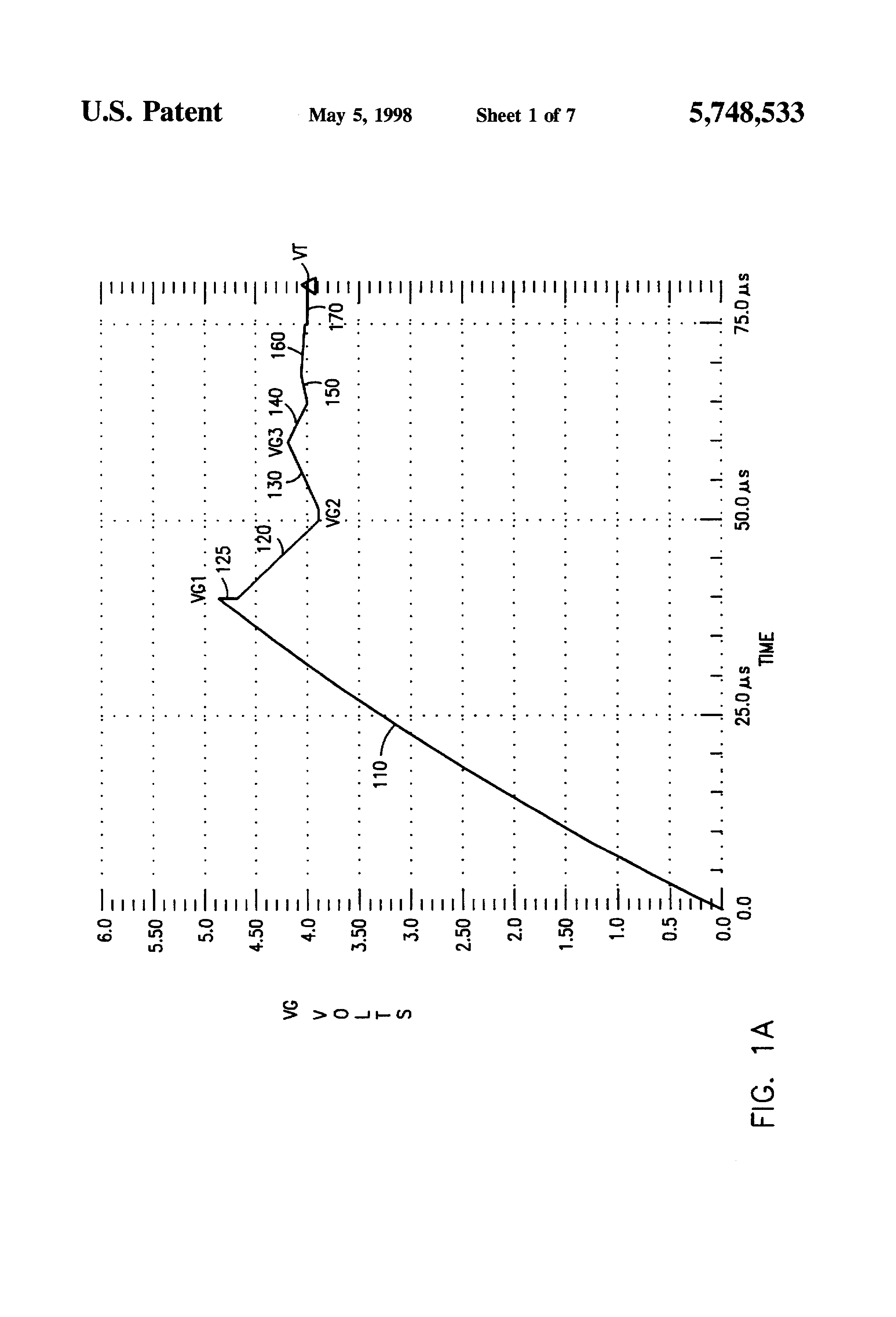
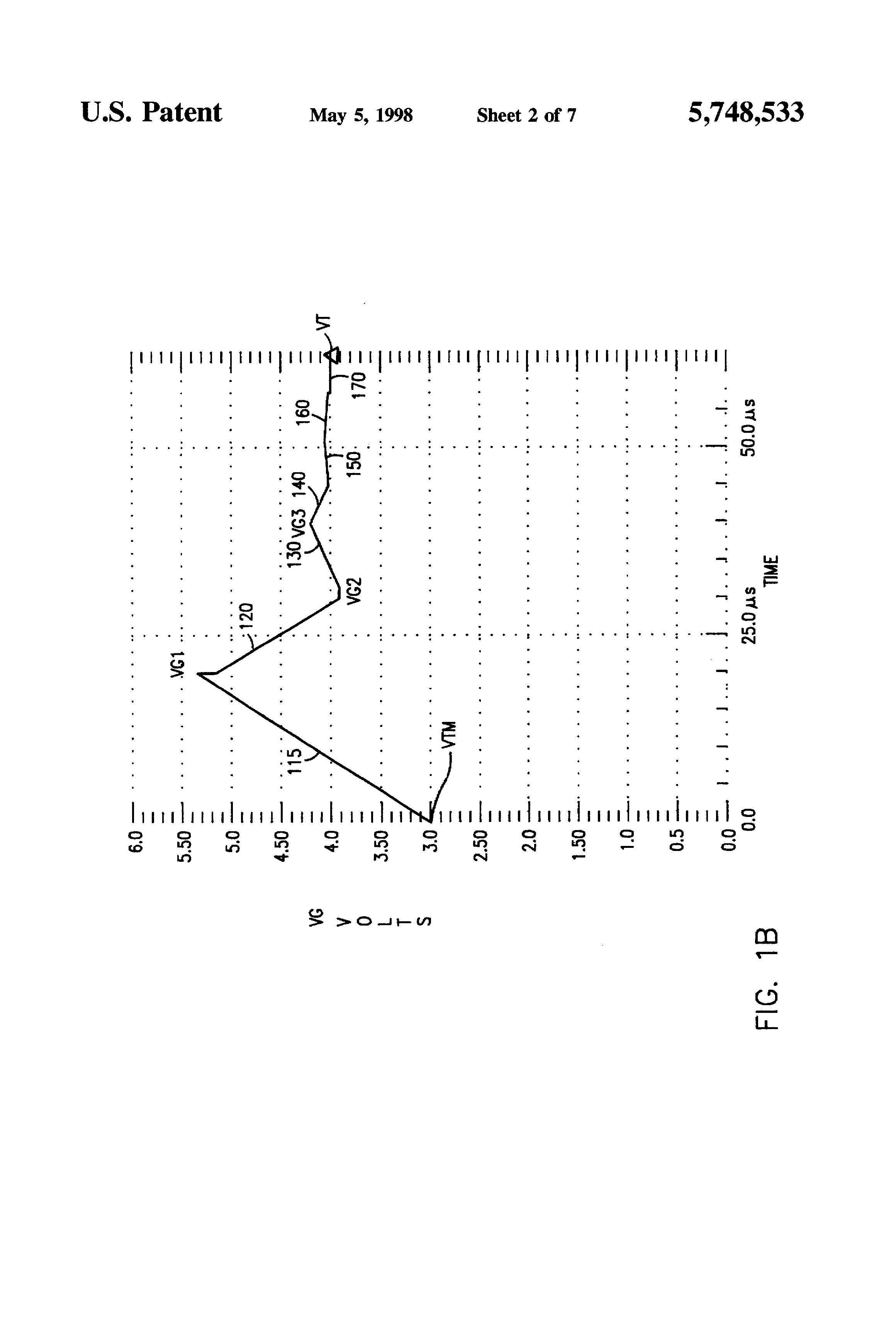
FIGS. 1A and 1B show plots of gate voltages applied to a transistor when using read processes in accordance with embodiments of the invention to read the threshold voltage of the transistor.

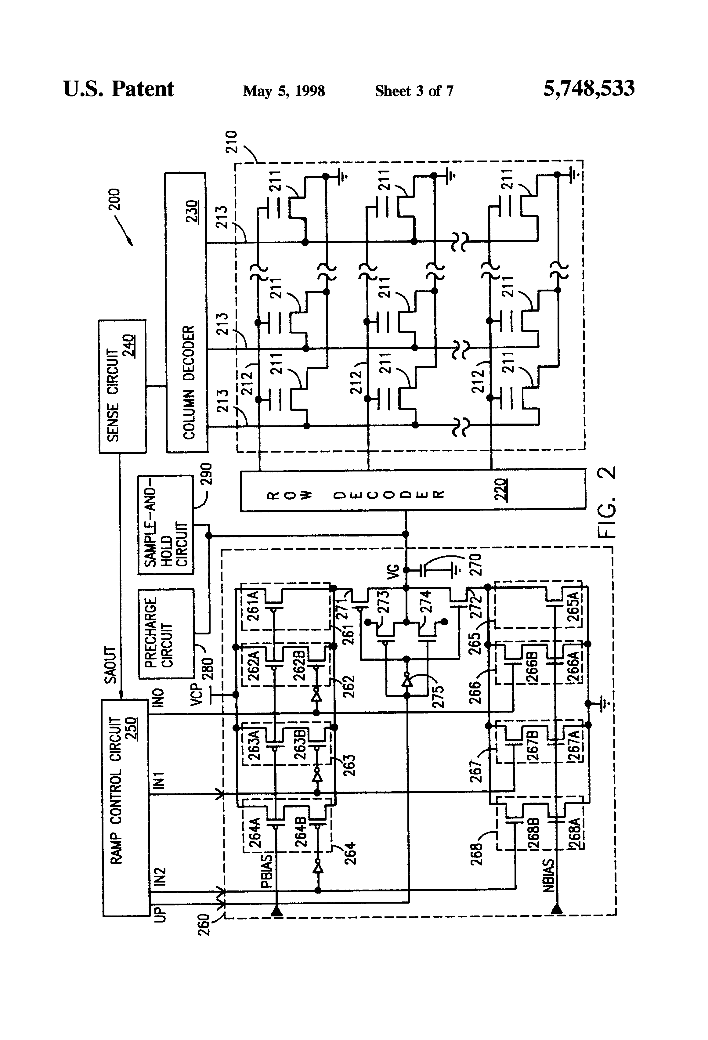
FIG. 2 shows a portion of a memory in accordance with an embodiment of the invention.

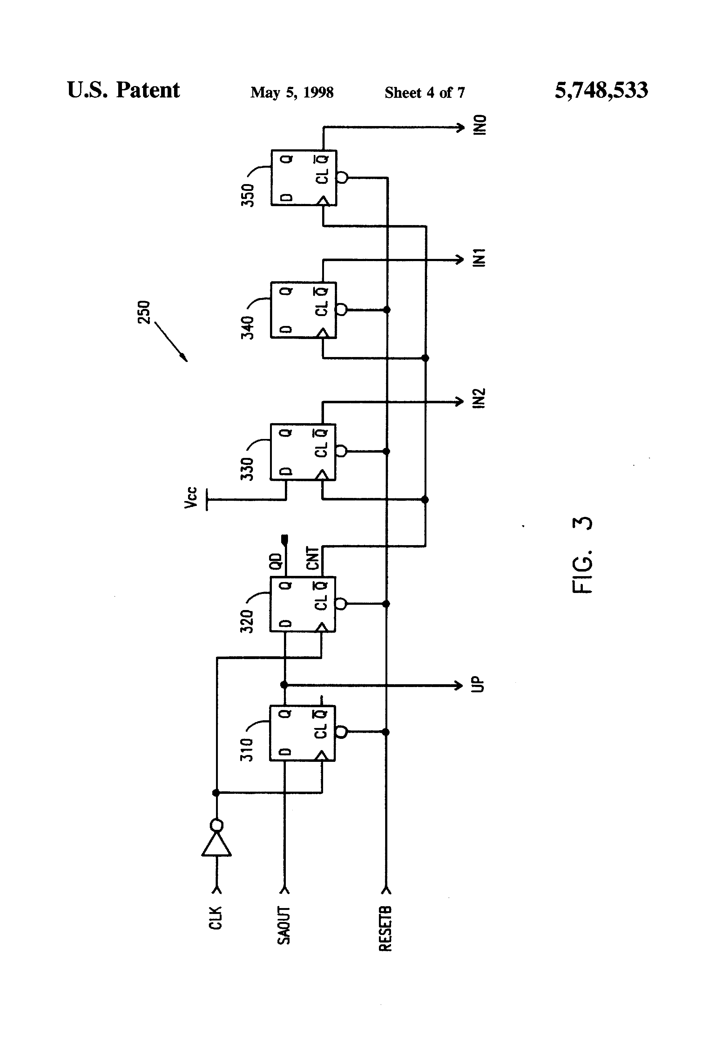
FIG. 3 shows a ramp control circuit for a read circuit in the memory shown in FIG. 2.

FIG. 4 shows timing diagrams for signals generated in the ramp control circuit of FIG. 3.

FIGS. 5 and 6 shows portions of other memories in accordance with embodiments of the invention.

Use of the same reference symbols in different figures indicates similar or identical items.

DETAILED DESCRIPTION OF THE PREFERRED EMBODIMENTS

In accordance with an aspect of the invention, a method for reading the threshold voltage of a transistor proceeds in a series of stages. Each stage ramps (i.e. changes) the transistor's gate voltage in a direction and at a rate or rates selected for the stage and ends after the change in gate voltage causes the transistor to cross a trip point where the transistor turns on or off. The direction and magnitude of ramping are selected so that each stage ramps the gate voltage in the opposite direction from the preceding stage and ramp rates in later stages are generally lower than ramp rates in the earlier stages.

FIG. 1A shows an example of an N-channel transistor's gate voltage VG during a coarse-to-fine search process which reads the transistor. Read processes for P-channel are similar and will be apparent in view of the following description. Initially, gate voltage VG and a source voltage VS for the transistor are zero, and the transistor is off. During a first stage 110 of the read process, gate voltage VG is ramped up at a rate of about 1.4×10⁵ volts/second. A constant current of about 2.0 μA applied to a total capacitance of 14 pF, for example, would ramp up the gate voltage at 1.4×10⁵ volts/second. When gate voltage of the transistor passes the threshold voltage VT of the transistor the transistor turns on. Stage 110 continues until the after the turning on of the transistor is sensed. Accordingly, gate voltage VG continues moving up during a finite response time required to sense the transistor turning on and overshoots the trip point and the threshold voltage VT by an amount that depends on the ramping rate and the sensing time. The gate voltage VG ends stage 110 at a voltage VG1 which is greater than threshold voltage VT.

A second stage of the read process 120 begins when stage 110 ends. During stage 120, gate voltage VG is ramped down. When gate voltage VG is below threshold voltage VT, the transistor turns off (trips again). Stage 120 ends when tripping of the transistor is sensed which occurs after the gate voltage crosses the threshold voltage of the transistor. In the process illustrated in FIG. 1, stage 120 ramps gate voltage VG down at about the same rate that voltage VG was ramped up during first stage 110, about 1.4×10⁵ volts/second. However, in stage 120, the delay between tripping and sensing may be less than the delay in stage 110 because during stage 120, a sense circuit is charged to a level closer to the trip point. If the sensing time is decreased for stage 120, stage 120 ends at a gate voltage VG2 which is closer to threshold voltage VT than is voltage VG1.

During a third stage 130, ramping is reversed in direction from the preceding stage 120 and reduced in magnitude to about 7×10⁴ volts/second. The slower ramping during stage 130 when compared to stage 110 and 120 provides less overshoot than occurred during stages 110 and 120, and a gate voltage VG3 at the end of stage 130 is closer to threshold voltage VT than is gate voltage VG1 or VG2.

Subsequent stages 140, 150, 160, and 170 each reverses ramp direction from the preceding stage 130, 140, 150, and 160 respectively. The later stages uses lower ramp rates and end at gate voltages which converge on the trip point for the transistor. Stage 170, which is the last stage, uses the lowest ramp rate less than about 2×10⁴ volts/second. An advantage of the read process shown in FIG. 1A is that the final reading has an accuracy which is determined by the ramp rate of stage 170. However, during the preceding stages, higher ramp rates more quickly drive gate voltage VG to the threshold level. Accordingly, the read process of FIG. 1A can take considerably less time than a read process which used a constant ramp rate equal to the ramp rate of step 170.

In the process of FIG. 1A, the ramp rate is reduced by about half about every other stage. An alternative process reduces the ramp rate each stage. However, many patterns for reducing ramp rates may be employed. For example, the ramp rate may be reduced proportionally for each successive stage, for example, by one half, one third, or one fourth, or reduced irregularly with large (or small) reductions in early stages and small (or large) reductions in late stages. Additionally, the ramp rate may be changed during a stage. Alternatively, the ramp rate is held constant which causes the gate voltage to oscillate around the trip point being read, and a filter is used to extract the trip point from the oscillating signal. As still another alternative, ramping is stopped entirely after a stage which determines the trip point to a desired accuracy, and capacitance in the system holds the measured voltage for later sampling.

Ideally, ramp rate reductions are selected to minimize the read time required to provide the desired accuracy. Minimization of read time depends on the starting point of the gate voltage, the range of possible threshold voltages which can be read, the maximum usable ramp rate, the minimum ramp rate (i.e. the desired accuracy), and the times required to sense the ends of the stages.

In a worst case for the processes of FIG. 1A, first stage 110 ramps gate voltage VG from 0 volts to the highest possible threshold voltage, for example up to 6 volts. The worst case provides the longest read time and increases the amount of time which must be allotted for each read. FIG. 1B shows a read process which reduces the worst case read time. In the process of FIG. 1B, gate voltage VG is initially charged to a voltage level VTM which is the mean of possible threshold voltages or trip points. The initial charging of gate voltage VG to voltage level VTM may be done quickly using a power supply. Once the gate is initially charged, whether the transistor conducts at voltage VTM is sensed, and a ramping direction for a first stage 115 is selected to drive voltage VG toward the trip point. In FIG. 1B, threshold voltage VT is greater than voltage VTM so that the transistor initially does not conduct and ramping up is selected for stage 115. If the transistor initially conducted, stage 115 would ramp gate voltage VG down.

Starting the process at voltage VTM, the middle of the range of possible ending gate voltages, reduces the average and the worst case read times because the maximum difference between VTM and a possible threshold voltage is half the range of possible threshold voltages and initial ramping stage 115 takes less time. After the initial stage 115, the read process of FIG. 1B proceeds as described above for the process of FIG. 1A.

FIG. 2 shows a portion of an analog memory 200 which includes a read circuit in accordance with an embodiment of the invention. Memory 200 contains an array 210 of N rows and M columns of memory cells 211 which a row decoder 220 and a column decoder 230 connect to the read circuit during a read. The read circuit includes a sense circuit 240, a ramp control circuit 250, and a word line driver 260. Write circuits and input/output interfaces which are components of memory 200 are well known in the art and are not shown in FIG. 2. Memory cells 211 can be floating gate transistors, metal nitride oxide silicon (MNOS) transistors, or split gate memory cells, each having a single accessible gate and a threshold voltage which indicate a value stored. Alternative embodiments of the invention employ multiple transistor memory cells which have separate select gates (not shown) and control gates.

In still other alternative embodiments, memory 200 is a multilevel memory which stores multiple bits of information in each memory cell 211. A multilevel memory provides a digital-to-analog conversion when writing a digital value as a threshold voltage of a memory cell, and an analog-to-digital conversion of a threshold voltage read from a memory cell.

Each word line 212 in memory array 210 is connected to the control gates of a row of memory cells 211 and to row decoder 220. When reading a selected one of memory cells 211, row decoder 220 connects word line driver 260 to a selected one of word lines 212 which is connected to the control gate of the selected memory cell. The remaining unselected word lines are grounded. Row decoders such as row decoder 220 which select a row indicated by an address signal are well known in the art.

Initially, the selected word line is charge to the desired starting point of the search by a precharge circuit 280. The starting point of the search may be the lowest possible threshold voltage, the midpoint of the range of possible threshold voltages, the highest possible threshold voltage, the ground potential, the supply voltage Vcc, or any other desired voltage. In a first stage of a coarse-to-fine search, word line driver 260 ramps a voltage VG, the voltage on the selected word line, towards the threshold voltage of the selected memory cell. Memory cells 211 are N-channel devices having source lines which are grounded, so that when voltage VG is greater than the threshold voltage of the selected memory cell the selected memory cell turns on.

Each bit line 213 in memory array 210 is connected to the drains of a column of memory cells 211 and to column decoder 230. During reading of the selected memory cell, column decoder 230 connects sense circuit 240 to a selected one of bit lines 213 which is connected to the drain of the selected memory cell. Sense circuit 240 senses whether any memory cell 211 connected to the selected bit line conducts. A digital signal SAOUT from sense circuit 240 is high if no memory cell connected to the selected bit line conducts and low if sense circuit 240 senses that the selected memory cell conducts.

Ramp control circuit 250 monitors signal SAOUT. When signal SAOUT is high, ramp control circuit 250 asserts a signal UP, and word line driver 260 ramps up voltage VG. When signal SAOUT is low, ramp control circuit 250 deasserts a signal UP, and word line driver 260 ramps down voltage VG. Accordingly, each time the selected memory cell trips, sense circuit 240 changes signal SAOUT and word line driver 260 reverses the direction of ramping.

In memory 200, word line driver 260 contains pull-up circuits 261 to 264 which a P-channel transistor 271 connects to a capacitor 270 when signal UP is asserted. Capacitor 270 is added to slow the ramping rate and typically has a capacitance of about 10 to 100 pF which dominates a typical word line capacitance of a few pF. An N-channel transistor 272 connects pull-down devices 265 to 268 to capacitor 270 when signal UP is deasserted.

At the end of each stage in a read process, signal UP switches from high to low or low to high. This switching can cause a rapid change in voltage VG because changes in signal UP pass through the gate capacitance of transistors 271 and 272. For example, in FIG. 1A, the beginning of stage 120 includes a rapid drop 125 in the gate voltage caused by signal UP dropping from supply voltage Vcc to ground. In word line driver 260, transistors 273 and 274 have gate voltages which are complementary to the gate voltages of transistors 271 and 272 so that switching of the gate voltages of transistors 273 and 274 oppose changes caused by switching of the gate voltages of transistors 271 and 272. The gate capacitance of transistors 273 and 274 can be selected to match respective transistors 271 and 272, to nearly eliminate changes in voltage VG caused by changing signal UP.

The magnitude of the current which charges or discharges capacitor 270 depends on which of pull-up circuits 261 to 264 or pull-down circuits 265 to 268 are disabled. Ramp control circuit 250 generates signals IN0, IN1, and IN2 to selectively disable none, some, or all of pull-up circuits 262 to 264 or pull-down circuits 266 to 268. When signals UP, IN0, IN1, and IN2 enable all of pull-up circuits 261 to 264, voltage VG ramps up at a maximum rate controlled which is the sum of the currents through pull-up circuits 261 to 264. If signal Up is deasserted and all of pull-down circuits 265 to 268 are enabled, voltage VG ramps down at a maximum rate. In late stages of the read process, ramp control circuit 250 changes signals IN0, IN1, and IN2 to disable some or all of pull-up circuits 262 to 264 or pull-down circuits 266 to 268 and reduce the ramp rate.

The amount of current through each of circuits 261 to 268 depends on the size of P-channel transistors 261A to 264A and N-channel transistors 265A to 268A. P-channel transistors 261A to 264A are connected to a voltage VCP which is greater than the maximum threshold voltage of memory cells 211 and have bias voltage PBIAS applied to their gates. N-channel transistors 265A to 268A are connected to ground and have bias voltage NBIAS are applied to their gates. Each of circuits 262 to 264 and 266 to 268 is individually enabled or disabled by turning on or off a corresponding one of transistors 262B to 264B and 266B to 268B. Circuits 261 and 265 are enabled or disabled solely by transistors 271 and 272.

In one embodiment of the invention, pull-up circuit 261 is not present, and each pull-up circuit 262 to 264 supplies a different amount of current depending on the size of transistors 262A to 264A. For example, pull-up circuit 262 provides the smallest current, pull-up circuit 263 provides three times the current provided by pull-up circuit 262, and pull-up circuit 264 provides twelve times the current of pull-up circuit 262. If all of signals IN0, IN1, and IN2 are asserted high, a total current, which is sixteen times the current through pull-up circuit 262, ramps up the gate voltage VG. Deasserting signal IN2 drops the ramping rate by a factor of four, and deasserting signals IN2 and IN1 decreases the ramping rate by a factor of sixteen.

FIG. 3 shows an embodiment of ramp control circuit 250. Ramp control circuit 250 contains flip- flops 310, 320, 330, 340, and 350. Signal SAOUT from the sense circuit is applied to a data input terminal of flip-flop 310, and a non-inverted output terminal of flip-flop 310 is coupled to the data input terminal of flip-flop 320. A signal CLK clocks flip- flops 310 and 320. A signal CNT from an inverted output terminal of flip-flop 320 clocks flip- flops 330, 340, and 350 which are connected together with a non-inverted output terminal of flip-flop 330 coupled to a data input terminal of flip-flop 340 and a non-inverted output terminal of flip-flop 340 coupled to a data input terminal of flip-flop 350. Output signals UP, IN2, IN1, and IN0 are respectively from a non-inverted output terminal of flip-flop 310 and inverted output terminals of flip- flops 330, 340, and 350.

FIG. 4 shows timing diagrams of signals in ramp control circuit 250 of FIG. 3 during a read process which is begun at time 405 when a signal RESETB is asserted low to reset or clear flip- flops 310, 320, 330, 340, and 350. Resetting the flip-flops causes signals UP, IN2, IN1, and IN0 to be low, high, high, and high respectively so that word line driver 260 drives the selected word line toward ground. Sense circuit 240 is then activated and assets signal SAOUT high at time 415 to indicate that the selected memory cell does not conduct. At time 420, an edge of signal CLK triggers flip-flop 310 which asserts signal UP to begin ramping up voltage VG. Flip-flop 320 is also triggered at time 420, but signal CNT does not change because the signal at the data input terminal of flip-flop 320 at time 420 is low.

Ramping up continues until after time 425 when sense circuit 240 senses that the selected memory cell has tripped. In particular, at time 430, another edge of signal CLK triggers flip-flop 310 which deasserts signal UP to begin ramping down voltage VG. Flip-flop 320 deasserts signal CNT at time 430. Flip- flops 330, 340, and 350, being positive edge triggered, do not change signals IN2, IN1, or IN0 so that ramping down is still at the maximum ramp rate.

Ramping down continues until time 440 which is after sense circuit 240 senses that the selected memory cell has tripped again and when flip-flop 310 asserts signal UP to begin ramping up voltage VG. Flip-flop 320 asserts signal CNT at time 440 which triggers flip- flops 330, 340, and 350. Flip-flops 330 has its data input coupled to a supply voltage Vcc and when triggered deasserts signal IN2. Deasserting signal IN2 causes word line driver 260 to reduce the ramping rate. Signals IN1 and IN0 remain asserted at time 440 because signals at data input terminals of flip-flops are low. At time 450 which is the next edge of signal CLK, word line driver 260 is still ramping up voltage VG, and the selected memory cell does not conduct. Signal CLK triggers flip-flop 320 which deasserts signal CNT because signal UP changed at time 440.

Sense circuit 240 next senses that the selected memory cell trips at time 455; and at time 460, flip-flop 310 changes signal UP. Ramping down begins at the same rate as the previous ramping up stage because signals IN2, IN1, and IN0 do not change at time 460. Flip-flop 320 does not change signal CNT until time 470, the edge of signal CLK following the change in signal UP. At time 470, flip-flop 340 deasserts signal IN1, and the ramping rate falls.

For the timing diagram of FIG. 4, each stage of the read process ends at an edge of signal CLK following sense circuit 240 sensing that the selected memory cell has tripped. The ramping rate decreases one cycle of signal CLK after the beginning of each stage (except the first stage) until all of signals IN2, IN1, and IN0 are deasserted after which only pull-up circuit 261 or pull-down circuit 265 control gate voltage VG. Pull-up circuit 261 and pull-down circuit 265 may be designed to provide and draw only a minimal current which keeps gate voltage VG near the level found at the end of the stage in which signal IN0 was deasserted. In this way, if the total read time for each read is constant, the read voltage is retained for cases where the search process quickly converges on the voltage to be read. If desired, a filter extracts an average value from voltage VG while voltage VG oscillates around the trip point.

A sample-and-hold circuit 290 holds voltage VG found at the end of the read process. This voltage depends on the trigger point sensed by sense circuit 240 and may differ somewhat from the threshold voltage of the selected cell. FIG. 5 shows an example memory 500 which illustrates the difference between the threshold voltage and the trip point of a memory cell. Memory 500 contains an array 210 of memory cells 211, a row decoder 220, a word line driver 260, and a ramp control circuit 250 which operate as described above in regard to FIG. 2. The sense circuit in memory 500 includes an amplifier 545, a reference cell 511, and transistors 542, 543, 544, 546 and 547 which forms a circuit such that at the trip point a current through the selected memory cell is equal to a current through reference cell 511.

Reference cell 511 is structurally identical to memory cells 211 and is part of a row of reference cells. The reference cells may be formed in the same area as array 210 and with the same spacing as memory cells 211 so that the reference cells are subject to substantially the same process variations as are memory cells 211. The reference cells differ from memory cells 211 in that the control gates of the reference cells are not coupled to word lines 212, and a bit line 513 which connects to the drains of the reference cells is not selectable by column decoder 530.

During a read of a selected memory cell, a reference voltage VREF which is slightly greater than the threshold voltage of reference cell 511 is applied to the control gate of reference cell 511, and a drain voltage is applied to the bit line connected to the drain of the reference cell so that a current flows through reference cell 511. Preferably the current is small on the order of 1 μA for a typical analog memory cell structure. A cascading device 547 which has a gate voltage fixed by a second reference VBIAS may be used to control the drain voltage. VBIAS would typically be about 2 volts to limit the drain voltage and prevent read disturb of reference cells 511. Transistor 542 is turned on to apply the drain voltage to the reference cell 511.

At the trip point, the current through reference cell 511 is equal to the current through the selected memory cell. To accomplish this, a current mirror is created using a transistor 543 connected in series with transistors 542 and 547 and reference cell 511. The gate and drain of transistor 543 are coupled to the gate of a transistor 544 which is connected in series with a cascading device 546, a transistor 531 which is turned on inside a column decoder 530, and the selected memory cell. Transistor 544 is identical to transistor 543. Cascoding devices 546 and 547 are identical and have the same gate voltage (VBIAS), and transistor 542 is identical to the transistor 531 which is turned on in column decoder to connect the sense circuit to the selected cell.

Amplifier 545 is connected to nodes in both sides of the current mirror. When the current through the selected memory cell is not equal to the current through reference cell 511, the current mirror is unbalanced. For example, if the selected memory cell conducts less current than reference cell 511, voltages at a positive input terminal 544 of amplifier 545 is higher than voltage at a negative input terminal 549 of amplifier 545, and amplifier 545 drives signal SAOUT high. If the selected memory cell conducts more current than reference cell 511, voltages at positive input terminal 548 is lower than voltage at negative input terminal 549, and amplifier 545 deasserts signal SAOUT.

The trip point of the sense circuit of FIG. 5 is the point where currents are equal. At the trip point, word line voltage VG for the selected memory cell is greater than the threshold voltage of the selected memory cell by the same amount that reference voltage VREF is greater than the threshold voltage of reference cell 511. Typically, voltage VG being different from the threshold voltage is unimportant because during reading the relative threshold voltages of the memory cells, rather than the absolute threshold voltages, indicate the values stored in the memory cells, and voltage VG indicates the relative threshold voltage.

FIG. 6 shows a memory 600 including reference cells 611 having control gates connected to word lines 212. In accordance with one embodiment of the invention, reference cells 611 are unprogrammed, i.e. have the lowest possible threshold voltage. During a read, word line driver 260 applies gate voltage VG to both the selected memory cell and to a reference cell 611 in the same row as the selected memory cell. When ramping up voltage VG, the reference cell begins to conduct before the selected memory cell begins to conduct unless the selected memory cell also has the lowest threshold voltage. Voltage on positive input terminal 548 is near supply voltage Vcc when the selected memory cell does not conduct, and voltage at negative input terminal 549 is lower because a current passes through transistor 643. Amplifier 545 provides a high output when transistor 211 does not conduct.

When voltage VG nears the threshold voltage of the selected memory cell, the selected memory cell begins to conduct and the voltage at positive input terminal 548 drops. Voltage at negative input terminal 549 also drops because the conducting reference cell conducts more current as voltage VG increases. However, transistor 643 is bigger (e.g. has a larger channel width) than transistor 544 so that the increase in current through the selected memory cell causes voltage on the positive input terminal 548 to drop faster than the voltage on the negative input terminal 549 when the selected memory cell begins to conduct. When ramping down voltage VG, the selected memory cell begins to turn off, and voltage at positive input terminal 548 rises faster than voltage at negative input terminal 549.

In the memory 600, current through a memory cell at the trip point for the memory cell depends on the threshold voltage of the memory cell. When higher threshold voltage memory cells are read, higher currents flow through both the reference cell and the selected memory cell because voltage VG provides greater overdrive to the reference cell. Accordingly, the difference between the trip point and the threshold voltage for a cell increases with higher threshold voltages. This make determination of the absolute threshold voltage more difficult, but voltage VG still provides an accurate measure of the relative threshold voltages of memory cells. An advantage of memory 600 is that reference cells can more easily be made as part of array 210 without the need to isolate the control gates of the reference cells or provide reference voltage for the control gates of the reference cells. Additionally, extra decode circuitry is not required to select a reference in the same row as the cell being read.

Although the present invention has been described with reference to particular embodiments, the description is only an example of the invention's application and should not be taken as a limitation. Various adaptations and combinations of features of the embodiments disclosed are within the scope of the present invention as defined by the following claims.
Claims (25)

  1. A read circuit comprising: a driver which is operable in a first mode to ramp up an output voltage which is applied to a gate in a selected memory cell during a read process and operable in a second mode to ramp down the output voltage which is applied to the gate in the selected memory cell during the read process; a sense circuit which generates a first signal indicating whether the selected memory cell conducts a first current; and a control circuit coupled to the sense circuit and the driver, wherein during the read process, the control circuit switches the driver between the first mode and second mode in response to changes in the first signal from the sense circuit.
  2. The read circuit of claim 1, further comprising a sample-and-hold circuit coupled to sample the output voltage of the driver, wherein a sample taken by the sample-and-hold circuit indicates a value read by the read circuit.
  3. The read circuit of claim 1, wherein: the driver comprises circuitry for ramping the output voltage at different rates; and the control circuit comprises circuitry for selecting that the driver ramp the output voltage at a first rate during a stage in a read process and ramp the output voltage at a second rate at an end of the read process, the second rate being lower than the first rate.
  4. The read circuit of claim 3, further comprising a sample-and-hold circuit coupled to sample the output voltage of the driver at the end of the read process, wherein a sample taken by the sample-and-hold circuit indicates a value read by the read circuit.
  5. The read circuit of claim 1, wherein the driver comprises: a first plurality of loads coupled to a voltage source; a second plurality of loads coupled to ground; a capacitor coupled to an output terminal which provides the output voltage; and selection circuitry which connects selected loads from the first and second pluralities to the output terminal, wherein a rate and direction of ramping of the output voltage depends on which loads are connected to the output terminal.
  6. The read circuit of claim 1, further comprising a row decoder coupled between the driver and an array of memory cells, and a column decoder coupled between the sense circuitry and the array.
  7. The read circuit of claim 1, wherein the sense circuit comprises: a reference cell which is structurally identical to the selected memory cell; a first bias circuit which biases the reference cell to conduct a reference current, the first bias circuit containing a first node; a second bias circuit which biases a source and a drain in the selected memory cell so that when the selected memory cell conducts the first current, a voltage on a second node in the second bias circuit is equal to a voltage on the first node in the first bias circuit; and a differential amplifier having a first input terminal coupled to the first node and a second input terminal coupled to the second node, wherein the differential amplifier generates the first signal.
  8. The read circuit of claim 7, wherein: the first bias circuit comprises a first transistor coupled between a supply voltage and a current carrying terminal of the reference cell; and the second bias circuit comprises a second transistor coupled between the supply voltage and a current carrying terminal of the selected memory cell, wherein a gate and drain of the first transistor are coupled to each other and to a gate of the second transistor to form a current mirror.
  9. The read circuit of claim 8, wherein: the first bias circuit further comprises a reference voltage generator which applies a reference voltage to a gate of the reference cell; the first transistor is structurally identical to the second transistor; and the first current is equal to the reference current.
  10. The read circuit of claim 8, wherein: the output voltage of the driver is applied to a gate of the reference cell; the reference cell has a threshold voltage that is at least as low as a lowest possible threshold voltage for the selected cell; the first transistor is larger than the second transistor; and the first current is smaller that the reference current.
  11. A memory comprising: an array of memory cells which includes word lines and bit lines, each word line being coupled to control gates of a row of memory cells in the array, each bit line being coupled to a column of memory cells in the array; a driver which is operable in a first mode to ramp up a voltage on a selected word line during a read process and operable in a second mode to ramp down the voltage on the selected word line during the read process; a sense circuit which generates a sense signal indicating whether a selected bit line conducts a first current; and a control circuit coupled to the sense circuit and the driver, wherein during the read process, the control circuit switches the driver between the first mode and second mode in response to changes in the sense signal.
  12. The memory of claim 11, wherein: the driver comprises circuitry for ramping the voltage on the selected word line, at different rates; and the control circuit comprises circuitry for selecting that the driver ramp the output voltage at a first rate during a stage of the read process and ramp the output voltage at a second rate at an end of the read process, the second rate being lower than the first rate.
  13. The memory of claim 12, further comprising a sample-and-hold circuit coupled to sample the voltage from the driver, wherein a sample taken at the end of the read process, by the sample-and-hold circuit indicates a value read by the read circuit.
  14. The memory of claim 11, further comprising: a row decoder coupled between the driver and the word lines, wherein during the read process, the row decoder connects the driver to the selected word line; and a column decoder coupled between the sense circuitry and the bit lines, wherein during the read process, the column decoder connects the sense circuit to a selected bit line.
  15. The memory of claim 11, wherein the memory stores analog values, each analog value being indicated by a threshold voltage of a memory cell in the array.
  16. The memory of claim 11, wherein the memory stores digital values, wherein a threshold voltage of a memory cell in the array indicates multiple bits for a stored digital value.
  17. The memory of claim 11, wherein the sense circuit comprises: a reference column which is in the array and contains memory cells having a lowest possible threshold voltage for memory cells in the array; a first bias circuit which during the read process is connected to a bit line for the reference column; a second bias circuit which during the read process is connected to the selected bit line; and a differential amplifier having a first input terminal and a second terminal respectively coupled to a first node in the first bias circuit and a second node in the second bias circuit, wherein the differential amplifier generates the sense signal.
  18. The memory of claim 17, wherein: the first bias circuit comprises a first transistor coupled between a supply voltage and the bit line for the reference column; and the second bias circuit comprises a second transistor coupled between the supply voltage and the selected bit line, wherein a gate and drain of the first transistor are coupled to each other and to a gate of the second transistor so that current on the bit line for the reference column controls the conductivity of the second transistor.
  19. The memory of claim 18, wherein the first transistor is larger than the second transistor.
  20. A method for reading a memory cell, the method comprising: executing a series of stages including a first stage and a last stage, wherein each stage comprises: changing a gate voltage applied to the memory cell; and ending the stage after changing of the gate voltage causes the memory cell to trip, wherein for each stage except the first stage, a direction selected for changing the gate voltage during the stage is opposite to a direction selected for changing the gate voltage during a preceding stage; sampling the gate voltage after the last stage; and determining from a sampled gate voltage a value read from the memory cell.
  21. The method of claim 20, wherein a rate of change in the gate voltage during the last stage is less than a rate of change in the gate voltage during the first stage.
  22. The method of claim 20, wherein determining the value read comprises determining an analog value.
  23. The method of claim 20, wherein determining the value read comprises determining a multi-bit digital value represented by the sampled gate voltage.
  24. The method of claim 20, further comprising: precharging the gate voltage of the selected memory cell to an initial level; sensing whether the initial level of the gate voltage causes the selected memory cell to conduct; and selecting a direction for changing the gate voltage during the first stage, wherein the direction selected for the first stage is determined by whether the initial level of the gate voltage causes the selected memory cell to conduct.
  25. The method of claim 24, wherein the initial level is a voltage which is the median of a range of possible threshold voltages for the selected memory cell.

Publications

Related applications (6)

  1. US08/622,332

    Priority application

  2. EP97301762A

    Priority application

  3. DE69717525T

    Priority application

  4. JP6989497A

    Priority application

  5. US08/622,332

    Claims priority

  6. US08/622,332

    Patent family

Record timeline

  1. Application filed by Invoice Technology Inc

  2. Assigned to INVOICE TECHNOLOGY, INC.

  3. Priority to US08/622,332

  4. Priority to EP97301762A

  5. Priority to DE69717525T

  6. Priority to JP6989497A

  7. Publication of US5748533A

  8. Application granted

  9. Assigned to INVOX TECHNOLOGY

  10. Assigned to SANDISK CORPORATION

  11. Assigned to SANDISK TECHNOLOGIES INC.

  12. Anticipated expiration

  13. Assigned to SANDISK TECHNOLOGIES LLC

  14. Expired - LifetimeCurrent

Legal events

  1. AS

    Assignment

    Owner name: INVOICE TECHNOLOGY, INC., CALIFORNIA

    Free format text: ASSIGNMENT OF ASSIGNORS INTEREST;ASSIGNORS:DUNLAP, FRANK;SO, HOCK C,;WONG, SAU C.;REEL/FRAME:007941/0279

    Effective date: 19960326

  2. STCF

    Information on status: patent grant

    Free format text: PATENTED CASE

  3. AS

    Assignment

    Owner name: INVOX TECHNOLOGY, CALIFORNIA

    Free format text: CHANGE OF NAME;ASSIGNOR:INVOICE TECHNOLOGY, INC.;REEL/FRAME:009436/0613

    Effective date: 19970623

  4. AS

    Assignment

    Owner name: SANDISK CORPORATION, CALIFORNIA

    Free format text: ASSIGNMENT OF ASSIGNORS INTEREST;ASSIGNOR:INVOX TECHNOLOGY;REEL/FRAME:011812/0888

    Effective date: 19990920

  5. REMI

    Maintenance fee reminder mailed

  6. FPAY

    Fee payment

    Year of fee payment: 4

  7. SULP

    Surcharge for late payment

  8. FPAY

    Fee payment

    Year of fee payment: 8

  9. FPAY

    Fee payment

    Year of fee payment: 12

  10. AS

    Assignment

    Owner name: SANDISK TECHNOLOGIES INC., TEXAS

    Free format text: ASSIGNMENT OF ASSIGNORS INTEREST;ASSIGNOR:SANDISK CORPORATION;REEL/FRAME:026224/0071

    Effective date: 20110404

  11. AS

    Assignment

    Owner name: SANDISK TECHNOLOGIES LLC, TEXAS

    Free format text: CHANGE OF NAME;ASSIGNOR:SANDISK TECHNOLOGIES INC;REEL/FRAME:038807/0980

    Effective date: 20160516

Patent citations (2)

  1. US5128895A

    Method for programming a virtual ground EPROM cell including slow ramping of the column line voltage

    Intel Corporation · July 7, 1992 · Examiner cited

  2. US5487033A

    Structure and method for low current programming of flash EEPROMS

    Intel Corporation · January 23, 1996 · Examiner cited

Cited by (188)

  1. US7898868B2

    Multi-state memory

    Sandisk Corporation · March 1, 2011

  2. US6868006B2

    Clock synchronized non-volatile memory device

    Renesas Technology Corp. · March 15, 2005

  3. US6768672B2

    Clock Synchronized Non-Volatile Memory Device

    Renesas Technology Corp. · July 27, 2004

  4. US20070064483A1

    Clock synchronized non-volatile memory device

    Hitoshi Miwa · March 22, 2007 · Examiner cited

  5. US7193894B2

    Clock synchronized nonvolatile memory device

    Renesas Technology Corp. · March 20, 2007

  6. US6038165A

    Nonvolatile memory device and refreshing method

    Hitachi, Ltd. · March 14, 2000 · Examiner cited

  7. US7161830B2

    Clock synchronized nonvolatile memory device

    Renesas Technology Corp. · January 9, 2007

  8. US6751119B2

    Clock synchronized non-volatile memory device

    Renesas Technology Corp. · June 15, 2004

  9. US6111790A

    Non-volatile memory device and refreshing method

    Hitachi, Ltd. · August 29, 2000 · Examiner cited

  10. US20060198201A1

    Multi-bits storage memory

    Hitoshi Miwa · September 7, 2006 · Examiner cited

  11. US6166949A

    Nonvolatile memory device and refreshing method

    Hitachi, Ltd. · December 26, 2000 · Examiner cited

  12. US7324375B2

    Multi-bits storage memory

    Solid State Storage Solutions, Llc · January 29, 2008

  13. US7327604B2

    Clock synchronized non-volatile memory device

    Renesas Technology Corporation · February 5, 2008

  14. US6965525B2

    Clock synchronized nonvolatile memory device

    Renesas Technology Corp. · November 15, 2005

  15. US6226198B1

    Nonvolatile memory device and refreshing method

    Hitachi, Ltd. · May 1, 2001

  16. US6747941B2

    Clock synchronized non-volatile memory device

    Renesas Technology Corp. · June 8, 2004

  17. US20050162940A1

    Clock synchronized nonvolatile memory device

    Hitoshi Miwa · July 28, 2005 · Examiner cited

  18. US6912156B2

    Clock synchronized nonvolatile memory device

    Renesas Technology Corp. · June 28, 2005

  19. US6898118B2

    Clock synchronized non-volatile memory device

    Renesas Technology Corp. · May 24, 2005

  20. US7286397B2

    Clock synchronized nonvolatile memory device

    Renesas Technology Corporation · October 23, 2007

  21. US6850434B2

    Clock synchronized nonvolatile memory device

    Renesas Technology Corp. · February 1, 2005

  22. US5889698A

    Nonvolatile memory device and refreshing method

    Hitachi, Ltd. · March 30, 1999 · Examiner cited

  23. US6366495B2

    Nonvolatile memory device and refreshing method

    Hitachi, Ltd. · April 2, 2002

  24. US6847549B2

    Clock synchronized non-volatile memory device

    Renesas Technology Corp. · January 25, 2005

  25. US6829163B2

    Clock synchronized nonvolatile memory device

    Hitachi, Ltd. · December 7, 2004

  26. US6459614B1

    Non-volatile memory device and refreshing method

    Hitachi, Ltd. · October 1, 2002

  27. US6804147B2

    Clock synchronized non-volatile memory device

    Renesas Technology Corp. · October 12, 2004

  28. US20030035317A1

    Nonvolatile memory device and refreshing method

    Hitoshi Miwa · February 20, 2003 · Examiner cited

  29. US20040184317A1

    Clock synchronized nonvolatile memory device

    Hitoshi Miwa · September 23, 2004 · Examiner cited

  30. US20040179399A1

    Clock synchronized nonvolatile memory device

    Hitoshi Miwa · September 16, 2004 · Examiner cited

  31. US20040179384A1

    Clock synchronized nonvolatile memory device

    Hitoshi Miwa · September 16, 2004 · Examiner cited

  32. US20100020615A1

    Clock synchronized non-volatile memory device

    Hitoshi Miwa · January 28, 2010 · Examiner cited

  33. US20040179400A1

    Clock synchronized nonvolatile memory device

    Hitoshi Miwa · September 16, 2004 · Examiner cited

  34. US20040174743A1

    Clock synchronized nonvolatile memory device

    Hitoshi Miwa · September 9, 2004 · Examiner cited

  35. US20030147284A1

    Nonvolatile memory device and refreshing method

    Hitoshi Miwa · August 7, 2003 · Examiner cited

  36. US6751120B2

    Clock synchronized non-volatile memory device

    Renesas Technology Corp. · June 15, 2004

  37. US6757194B2

    Clock synchronized non-volatile memory device

    Renesas Technology Corp. · June 29, 2004

  38. US7542339B2

    Clock synchronized non-volatile memory device

    Solid State Storage Solutions, Llc · June 2, 2009

  39. US8804431B2

    Clock synchronized non-volatile memory device

    S4, Inc. · August 12, 2014

  40. US6256230B1

    Nonvolatile memory device and refreshing method

    Hitachi, Ltd. · July 3, 2001

  41. US6038167A

    Nonvolatile memory device and refreshing method

    Hitachi, Ltd. · March 14, 2000 · Examiner cited

  42. US6320785B1

    Nonvolatile semiconductor memory device and data writing method therefor

    Hitachi, Ltd. · November 20, 2001

  43. US5959882A

    Nonvolatile semiconductor memory device and data writing method therefor

    Hitachi, Ltd. · September 28, 1999 · Examiner cited

  44. US20030185056A1

    Nonvolatile semiconductor memory device and data writing method therefor

    Keiichi Yoshida · October 2, 2003 · Examiner cited

  45. US6906952B2

    Nonvolatile semiconductor memory device and data writing method therefor

    Renesas Technology Corp. · June 14, 2005

  46. USRE44350E1

    Nonvolatile semiconductor memory including multi-threshold voltage memory cells including voltage ranges indicating either an erase state or a two or more program state

    Renesas Electronics Corporation · July 9, 2013

  47. US6525960B2

    Nonvolatile semiconductor memory device including correction of erratic memory cell data

    Hitachi, Ltd. · February 25, 2003

  48. US5936892A

    Memory cell DC characterization apparatus and method

    Advanced Micro Devices, Inc. · August 10, 1999 · Examiner cited

  49. US20040246798A1

    Novel multi-state memory

    Guterman Daniel C. · December 9, 2004 · Examiner cited

  50. US20060034124A1

    Novel multi-state memory

    Sandisk Corporation · February 16, 2006 · Examiner cited

  51. US7573740B2

    Multi-state memory

    Sandisk Corporation · August 11, 2009

  52. US20080212374A1

    Novel Multi-State Memory

    Guterman Daniel C · September 4, 2008 · Examiner cited

  53. US7385843B2

    Multi-state memory

    Sandisk Corporation · June 10, 2008

  54. US20050248986A1

    High data rate write process for non-volatile flash memories

    Wong Sau C · November 10, 2005 · Examiner cited

  55. US7349255B2

    High data rate write process for non-volatile flash memories

    Sandisk Corporation · March 25, 2008

  56. US6038166A

    High resolution multi-bit-per-cell memory

    Invox Technology · March 14, 2000 · Examiner cited

  57. WO1999050853A1

    High resolution multi-bit-per-cell memory

    Invox Technology · October 7, 1999 · Examiner cited

  58. US5969986A

    High-bandwidth read and write architectures for non-volatile memories

    Invox Technology · October 19, 1999 · Examiner cited

  59. US6944058B2

    High data rate write process for non-volatile flash memories

    Sandisk Corporation · September 13, 2005 · Examiner cited

  60. US6137739A

    Multilevel sensing circuit and method thereof

    Hyundai Electronics Industries Co., Ltd. · October 24, 2000 · Examiner cited

  61. US20080049498A1

    Integrated Circuit with Analog or Multilevel Storage Cells and User-Selectable Sampling Frequency

    Werner Carl W · February 28, 2008 · Examiner cited

  62. US6184726B1

    Adjustable level shifter circuits for analog or multilevel memories

    Sandisk Corporation · February 6, 2001

  63. US20030202389A1

    Integrated circuit with analog or multilevel storage cells and user-selectable sampling frequency

    Sandisk Corporation, A Delaware Corporation · October 30, 2003 · Examiner cited

  64. US6760262B2

    Charge pump circuit adjustable in response to an external voltage source

    Sandisk Corporation · July 6, 2004

  65. US20030161171A1

    Adjustable charge pump circuit

    Invox Technology, A California Corporation · August 28, 2003 · Examiner cited

  66. US6370075B1

    Charge pump circuit adjustable in response to an external voltage source

    Sandisk Corporation · April 9, 2002

  67. US6185119B1

    Analog memory IC with fully differential signal path

    Sandisk Corporation · February 6, 2001

  68. US6549456B2

    Integrated circuit with analog or multilevel storage cells and user-selectable sampling frequency

    Sandisk Corporation · April 15, 2003

  69. US6556465B2

    Adjustable circuits for analog or multi-level memory

    Sandisk Corporation · April 29, 2003

  70. US20060256626A1

    Integrated Circuit with Analog or Multilevel Storage Cells and User-Selectable Sampling Frequency

    Werner Carl W · November 16, 2006 · Examiner cited

  71. US7298670B2

    Integrated circuit with analog or multilevel storage cells and user-selectable sampling frequency

    Sandisk Corporation · November 20, 2007

  72. US7554844B2

    Integrated circuit with analog or multilevel storage cells and user-selectable sampling frequency

    Sandisk Corporation · June 30, 2009

  73. US7106632B2

    Integrated circuit with analog or multilevel storage cells and user-selectable sampling frequency

    Sandisk Corporation · September 12, 2006

  74. EP1804251A3

    Techniques for analog and mutilevel storage using trimmable input voltage level shifter

    SanDisk Corporation · December 5, 2007 · Examiner cited

  75. US6169503B1

    Programmable arrays for data conversions between analog and digital

    Sandisk Corporation · January 2, 2001 · Examiner cited

  76. US6275417B1

    Multiple level flash memory

    Aplus Flash Technology, Inc. · August 14, 2001 · Examiner cited

  77. US6330185B1

    High bandwidth multi-level flash memory using dummy memory accesses to improve precision when writing or reading a data stream

    Multi Level Memory Technology · December 11, 2001

  78. US6278633B1

    High bandwidth flash memory that selects programming parameters according to measurements of previous programming operations

    Multi Level Memory Technology · August 21, 2001

  79. US6259627B1

    Read and write operations using constant row line voltage and variable column line load

    Multi Level Memory Technology · July 10, 2001

  80. US6558967B1

    Multi-bit-per-cell memory system with numbers of bits per cell set by testing of memory units

    Multi Level Memory Technology · May 6, 2003

  81. US6363008B1

    Multi-bit-cell non-volatile memory with maximized data capacity

    Multi Level Memory Technology · March 26, 2002

  82. US6856568B1

    Refresh operations that change address mappings in a non-volatile memory

    Multi Level Memory Technology · February 15, 2005

  83. US6522586B2

    Dynamic refresh that changes the physical storage locations of data in flash memory

    Multi Level Memory Technology · February 18, 2003

  84. US6396744B1

    Flash memory with dynamic refresh

    Multi Level Memory Technology · May 28, 2002

  85. US6754128B2

    Non-volatile memory operations that change a mapping between physical and logical addresses when restoring data

    Multi Level Memory Technology · June 22, 2004

  86. US7079422B1

    Periodic refresh operations for non-volatile multiple-bit-per-cell memory

    Samsung Electronics Co., Ltd. · July 18, 2006

  87. US6734719B2

    Constant voltage generation circuit and semiconductor memory device

    Kabushiki Kaisha Toshiba · May 11, 2004 · Examiner cited

  88. US6574158B1

    Method and system for measuring threshold of EPROM cells

    Cypress Semiconductor Corp. · June 3, 2003

  89. US20030137877A1

    Noise reduction technique for transistors and small devices utilizing an episodic agitation

    Nima Mokhlesi · July 24, 2003 · Examiner cited

  90. US20050057979A1

    Noise reduction technique for transistors and small devices utilizing an episodic agitation

    Nima Mokhlesi · March 17, 2005 · Examiner cited

  91. US7403421B2

    Noise reduction technique for transistors and small devices utilizing an episodic agitation

    Sandisk Corporation · July 22, 2008

  92. US6850441B2

    Noise reduction technique for transistors and small devices utilizing an episodic agitation

    Sandisk Corporation · February 1, 2005 · Examiner cited

  93. US7092292B2

    Noise reduction technique for transistors and small devices utilizing an episodic agitation

    Sandisk Corporation · August 15, 2006

  94. CN100520980C

    Noise reduction technique for transistors and small devices utilizing an episodic agitation

    桑迪士克股份有限公司 · July 29, 2009 · Examiner cited

  95. US20060239079A1

    Noise Reduction Technique for Transistors and Small Devices Utilizing an Episodic Agitation

    Nima Mokhlesi · October 26, 2006 · Examiner cited

  96. US20070170248A1

    Authentication Methods and Systems Including Embedded Auxiliary Data

    Brundage Trent J · July 26, 2007 · Examiner cited

  97. US20060198187A1

    Memory device with a ramp-like voltage biasing structure based on a current generator

    Stmicroelectronics S.R.L. · September 7, 2006 · Examiner cited

  98. US7359246B2

    Memory device with a ramp-like voltage biasing structure based on a current generator

    Stmicroelectronics S.R.L. · April 15, 2008 · Examiner cited

  99. US7554861B2

    Memory device with a ramp-like voltage biasing structure and reduced number of reference cells

    Daniele Vimercati · June 30, 2009 · Examiner cited

  100. US20060215463A1

    Memory device with a ramp-like voltage biasing structure and reduced number of reference cells

    Stmicroelectronics S.R.L. · September 28, 2006 · Examiner cited

  101. US20110225473A1

    Read operation for non-volatile storage with compensation for coupling

    Nima Mokhlesi · September 15, 2011 · Examiner cited

  102. US8427873B2

    Read operation for non-volatile storage with compensation for coupling

    Sandisk Technologies Inc. · April 23, 2013 · Examiner cited

  103. US8599611B2

    Distortion estimation and cancellation in memory devices

    Apple Inc. · December 3, 2013

  104. US8156403B2

    Combined distortion estimation and error correction coding for memory devices

    Anobit Technologies Ltd. · April 10, 2012

  105. US8570804B2

    Distortion estimation and cancellation in memory devices

    Apple Inc. · October 29, 2013

  106. US8239735B2

    Memory Device with adaptive capacity

    Apple Inc. · August 7, 2012

  107. US20080198650A1

    Distortion Estimation And Cancellation In Memory Devices

    Anobit Technologies Ltd. · August 21, 2008 · Examiner cited

  108. US8050086B2

    Distortion estimation and cancellation in memory devices

    Anobit Technologies Ltd. · November 1, 2011

  109. US20100131826A1

    Estimation of non-linear distortion in memory devices

    Anobit Technologies Ltd. · May 27, 2010 · Examiner cited

  110. US8060806B2

    Estimation of non-linear distortion in memory devices

    Anobit Technologies Ltd. · November 15, 2011

  111. USRE46346E1

    Reading memory cells using multiple thresholds

    Apple Inc. · March 21, 2017

  112. US8145984B2

    Reading memory cells using multiple thresholds

    Anobit Technologies Ltd. · March 27, 2012

  113. US8151163B2

    Automatic defect management in memory devices

    Anobit Technologies Ltd. · April 3, 2012

  114. CN101202108B

    Memory structure and operation method thereof

    旺宏电子股份有限公司 · June 2, 2010 · Examiner cited

  115. US8151166B2

    Reduction of back pattern dependency effects in memory devices

    Anobit Technologies Ltd. · April 3, 2012

  116. US8369141B2

    Adaptive estimation of memory cell read thresholds

    Apple Inc. · February 5, 2013

  117. US8429493B2

    Memory device with internal signap processing unit

    Apple Inc. · April 23, 2013

  118. US20100131827A1

    Memory device with internal signap processing unit

    Anobit Technologies Ltd · May 27, 2010 · Examiner cited

  119. US8234545B2

    Data storage with incremental redundancy

    Apple Inc. · July 31, 2012

  120. US8259497B2

    Programming schemes for multi-level analog memory cells

    Apple Inc. · September 4, 2012

  121. US20090043951A1

    Programming schemes for multi-level analog memory cells

    Anobit Technologies Ltd. · February 12, 2009 · Examiner cited

  122. US8174905B2

    Programming orders for reducing distortion in arrays of multi-level analog memory cells

    Anobit Technologies Ltd. · May 8, 2012

  123. US8068360B2

    Reading analog memory cells using built-in multi-threshold commands

    Anobit Technologies Ltd. · November 29, 2011

  124. US8527819B2

    Data storage in analog memory cell arrays having erase failures

    Apple Inc. · September 3, 2013

  125. US8270246B2

    Optimized selection of memory chips in multi-chips memory devices

    Apple Inc. · September 18, 2012

  126. US8769381B2

    Efficient re-read operations in analog memory cell arrays

    Apple Inc. · July 1, 2014

  127. US20090144600A1

    Efficient re-read operations from memory devices

    Anobit Technologies Ltd · June 4, 2009 · Examiner cited

  128. US8782497B2

    Efficient re-read operations in analog memory cell arrays

    Apple Inc. · July 15, 2014

  129. US8225181B2

    Efficient re-read operations from memory devices

    Apple Inc. · July 17, 2012

  130. US8209588B2

    Efficient interference cancellation in analog memory cell arrays

    Anobit Technologies Ltd. · June 26, 2012

  131. US20090157964A1

    Efficient data storage in multi-plane memory devices

    Anobit Technologies Ltd. · June 18, 2009 · Examiner cited

  132. US8085586B2

    Wear level estimation in analog memory cells

    Anobit Technologies Ltd. · December 27, 2011

  133. US8156398B2

    Parameter estimation based on error correction code parity check equations

    Anobit Technologies Ltd. · April 10, 2012

  134. US8230300B2

    Efficient readout from analog memory cells using data compression

    Apple Inc. · July 24, 2012

  135. US20090240872A1

    Memory device with multiple-accuracy read commands

    Anobit Technologies Ltd · September 24, 2009 · Examiner cited

  136. US8400858B2

    Memory device with reduced sense time readout

    Apple Inc. · March 19, 2013

  137. US8059457B2

    Memory device with multiple-accuracy read commands

    Anobit Technologies Ltd. · November 15, 2011 · Examiner cited

  138. US20100019832A1

    Self-Adaptive Multi-Stage Charge Pump

    Feng Pan · January 28, 2010 · Examiner cited

  139. US7969235B2

    Self-adaptive multi-stage charge pump

    Sandisk Corporation · June 28, 2011

  140. US8498151B1

    Data storage in analog memory cells using modified pass voltages

    Apple Inc. · July 30, 2013

  141. US8949684B1

    Segmented data storage

    Apple Inc. · February 3, 2015

  142. US8169825B1

    Reliable data storage in analog memory cells subjected to long retention periods

    Anobit Technologies Ltd. · May 1, 2012

  143. US8482978B1

    Estimation of memory cell read thresholds by sampling inside programming level distribution intervals

    Apple Inc. · July 9, 2013

  144. WO2010042820A1

    Differential threshold voltage non-volatile memory and related methods

    Arizona Board Of Regents, For And On Behalf Of Arizona State University · April 15, 2010 · Examiner cited

  145. US8488370B2

    Differential threshold voltage non-volatile memory and related methods

    Arizona Board Of Regents, A Body Corporate Of The State Of Arizona, Acting For And On Behalf Of Arizona State University · July 16, 2013

  146. US8462565B2

    Differential threshold voltage non-volatile memory and related methods

    Arizona Board Of Regents, A Body Corporate Of The State Of Arizona, Acting For And On Behalf Of Arizona State University · June 11, 2013

  147. US8239734B1

    Efficient data storage in storage device arrays

    Apple Inc. · August 7, 2012

  148. US8261159B1

    Data scrambling schemes for memory devices

    Apple, Inc. · September 4, 2012

  149. US8208304B2

    Storage at M bits/cell density in N bits/cell analog memory cell devices, M>N

    Anobit Technologies Ltd. · June 26, 2012

  150. US8248831B2

    Rejuvenation of analog memory cells

    Apple Inc. · August 21, 2012

  151. US8174857B1

    Efficient readout schemes for analog memory cell devices using multiple read threshold sets

    Anobit Technologies Ltd. · May 8, 2012

  152. US8397131B1

    Efficient readout schemes for analog memory cell devices

    Apple Inc. · March 12, 2013

  153. US8924661B1

    Memory system including a controller and processors associated with memory devices

    Apple Inc. · December 30, 2014

  154. US8228701B2

    Selective activation of programming schemes in analog memory cell arrays

    Apple Inc. · July 24, 2012

  155. US20100220509A1

    Selective Activation of Programming Schemes in Analog Memory Cell Arrays

    Anobit Technologies Ltd · September 2, 2010 · Examiner cited

  156. US8259506B1

    Database of memory read thresholds

    Apple Inc. · September 4, 2012

  157. US8832354B2

    Use of host system resources by memory controller

    Apple Inc. · September 9, 2014

  158. US8238157B1

    Selective re-programming of analog memory cells

    Apple Inc. · August 7, 2012

  159. US8479080B1

    Adaptive over-provisioning in memory systems

    Apple Inc. · July 2, 2013

  160. US8218392B2

    Word line driving apparatus

    Lapis Semiconductor Co., Ltd. · July 10, 2012 · Examiner cited

  161. US20110044122A1

    Word line driving apparatus

    Oki Semiconductor Co., Ltd. · February 24, 2011 · Examiner cited

  162. US8495465B1

    Error correction coding over multiple memory pages

    Apple Inc. · July 23, 2013

  163. US20110133820A1

    Multi-Stage Charge Pump with Variable Number of Boosting Stages

    Feng Pan · June 9, 2011 · Examiner cited

  164. US8677054B1

    Memory management schemes for non-volatile memory devices

    Apple Inc. · March 18, 2014

  165. US20110148509A1

    Techniques to Reduce Charge Pump Overshoot

    Feng Pan · June 23, 2011 · Examiner cited

  166. US8694814B1

    Reuse of host hibernation storage space by memory controller

    Apple Inc. · April 8, 2014

  167. US8572311B1

    Redundant data storage in multi-die memory systems

    Apple Inc. · October 29, 2013

  168. US8677203B1

    Redundant data storage schemes for multi-die memory systems

    Apple Inc. · March 18, 2014

  169. US8694853B1

    Read commands for reading interfering memory cells

    Apple Inc. · April 8, 2014

  170. US8572423B1

    Reducing peak current in memory systems

    Apple Inc. · October 29, 2013

  171. US8595591B1

    Interference-aware assignment of programming levels in analog memory cells

    Apple Inc. · November 26, 2013

  172. US9104580B1

    Cache memory for hybrid disk drives

    Apple Inc. · August 11, 2015

  173. US8767459B1

    Data storage in analog memory cells across word lines using a non-integer number of bits per cell

    Apple Inc. · July 1, 2014

  174. US8645794B1

    Data storage in analog memory cells using a non-integer number of bits per cell

    Apple Inc. · February 4, 2014

  175. US8856475B1

    Efficient selection of memory blocks for compaction

    Apple Inc. · October 7, 2014

  176. US8694854B1

    Read threshold setting based on soft readout statistics

    Apple Inc. · April 8, 2014

  177. US9021181B1

    Memory management for unifying memory cell conditions by using maximum time intervals

    Apple Inc. · April 28, 2015

  178. CN107025945A

    Memory system using nonlinear filtering scheme and reading method thereof

    三星电子株式会社 · August 8, 2017 · Examiner cited

  179. CN107025945B

    Memory system using non-linear filtering scheme and reading method thereof

    三星电子株式会社 · May 24, 2022 · Examiner cited

  180. WO2019240892A1

    Improved sense amplifier for a flash memory system

    Silicon Storage Technology, Inc. · December 19, 2019 · Examiner cited

  181. US11100975B2

    Semiconductor memory device and method for adjusting threthold voltage thereof

    Kioxia Corporation · August 24, 2021

  182. US11205480B1

    Ramp-based biasing in a memory device

    Micron Technology, Inc. · December 21, 2021 · Examiner cited

  183. US11769552B2

    Ramp-based biasing and adjusting of access line voltage in a memory device

    Micron Technology, Inc. · September 26, 2023

  184. US12603129B2

    Ramp-based biasing in a memory device

    Micron Technology, Inc. · April 14, 2026

  185. US11556416B2

    Controlling memory readout reliability and throughput by adjusting distance between read thresholds

    Apple Inc. · January 17, 2023

  186. US11847342B2

    Efficient transfer of hard data and confidence levels in reading a nonvolatile memory

    Apple Inc. · December 19, 2023

  187. CN117727349A

    storage array

    浙江力积存储科技有限公司 · March 19, 2024 · Examiner cited

  188. CN117727349B

    Storage Array

    浙江力积存储科技有限公司 · May 7, 2024 · Examiner cited

Related Patents