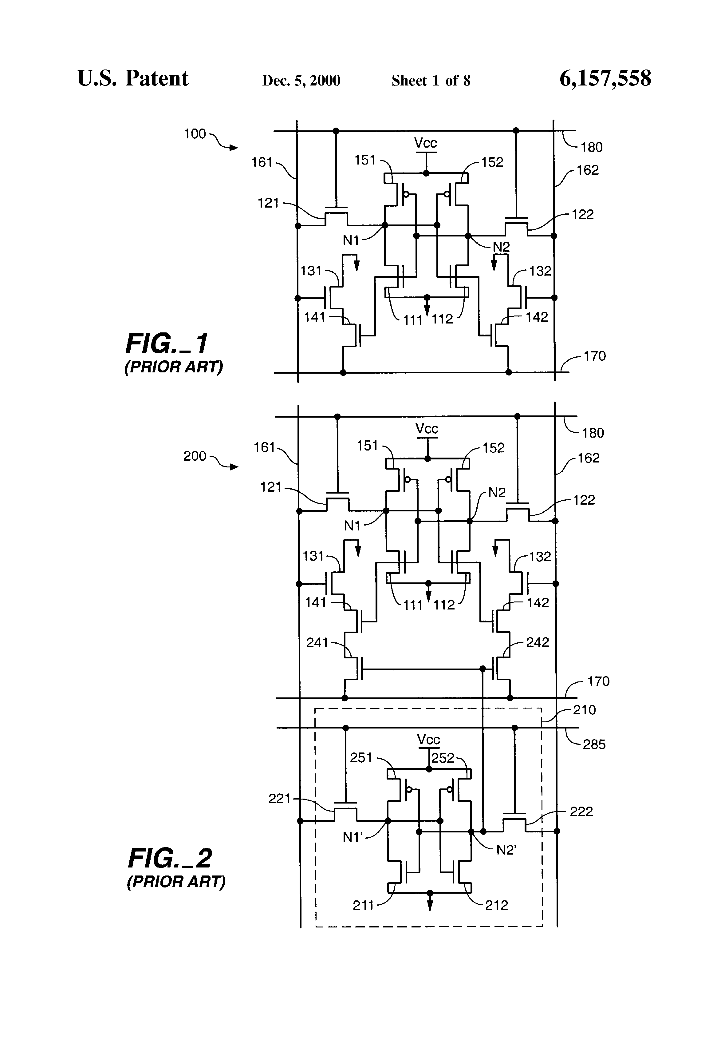
In accordance with an aspect of the invention, a transistor having a gate connected to a bit line replaces a pass transistor for writing to a CAM cell and replaces search transistors that are serially connected to change the state of a match line if there is no match during a search. These replacements permit removal of four transistors and a word line from an SRAM-based CAM cell and therefore provides a smaller and simpler CAM cell that can be less expensively integrated into an SRAM-based CAM.
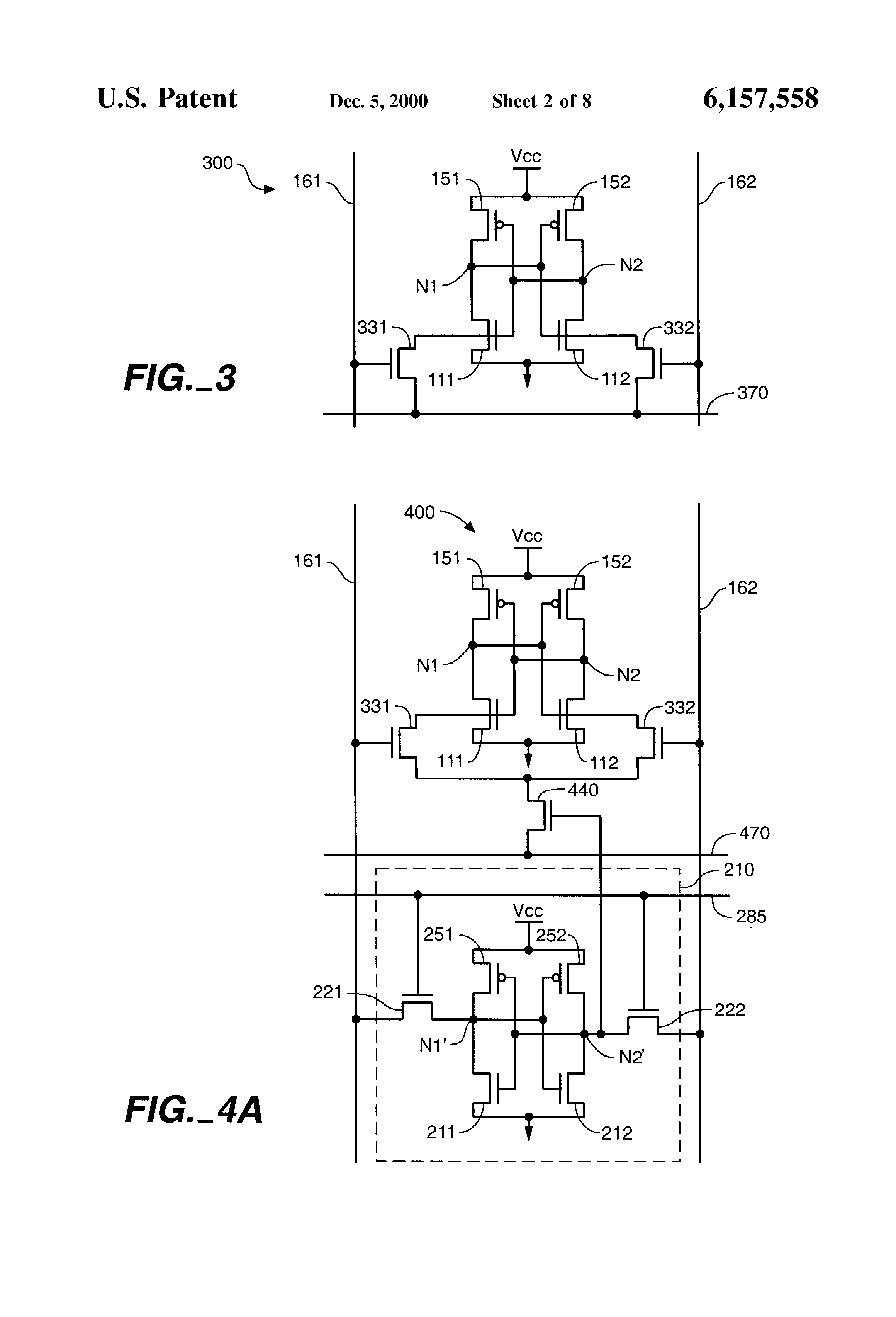
FIG. 3 shows an SRAM-based, binary CAM cell 300 in accordance with an embodiment of the invention. Binary CAM cell 300 is a six-transistor CMOS CAM cell including four N-channel field effect transistors 111, 112, 331, and 332 and two P- channel transistors 151 and 152. For a storage element in CAM cell 300, P-channel field effect transistor 151 and N-channel transistor 111 connect in series between a supply voltage Vcc and ground and have gates coupled to a node N2 between transistors 112 and 152. P-channel transistor 152 and N-channel transistor 112 also connect in series between supply voltage Vcc and ground but have gates coupled to a node N1 between transistors 151 and 111. CAM cell 300 does not have pass transistors or separate word and match lines. Instead, CAM cell 300 includes N- channel transistors 331 and 332 which connect a word/match line 370 to respective nodes N2 and N1. The gates of transistors 331 and 332 connect to bit lines 161 and 162 respectively.
A write operation, which stores a bit in CAM cell 300, applies complementary write signals to bit lines 161 and 162 to indicate the bit being written and grounds word/match line 370. The complementary write signals apply a voltage (e.g., supply voltage Vcc) to one bit line 161 or 162 and ground the other bit line 162 or 161. The voltage on bit line 161 or 162 turns on one transistor 331 or 332 so that the transistor 331 or 332 conducts. Grounding the other bit line 162 or 161 keeps the other transistor 332 or 331 off. The dimensions and charge mobility of transistors 331 and 332 are such that the saturation current through N- channel transistors 331 and 332 is greater than the saturation current through P- channel transistors 151 and 152. Accordingly, during a write, the conductive one of transistors 331 and 332 discharges the attached node N2 or N1 to the grounded word/match line 370. The node N2 or N1 being grounded turns on the opposite P- channel transistor 151 or 152 and turns off the opposite N- channel transistor 111 or 112 to pull the opposite node N1 or N2 up to supply voltage Vcc. The opposite node N1 or N2 being at the high voltage turns off P- channel transistor 152 or 151 and turns on N- channel transistor 112 or 111 to help pull down the first node N2 or N1 at the end of the write operation. At the end of the write operation, bit lines 161 and 162 are grounded before bringing word/match line 370 to a voltage near supply voltage Vcc. This allows transistors 111, 112, 151, and 152 to maintain the voltages on nodes N1 and N2, which represent the stored data bit. These biasing conditions prevail during standby or idle periods during which neither a search nor a write operation is taking place.
For illustration, the following description presumes that writing a one to CAM cell 300 places CAM cell 300 in a state where node N1 is nearly at supply voltage Vcc and node N2 is nearly at the ground potential. Correspondingly, writing a zero in CAM cell 300 places CAM cell 300 in a state where node N1 nearly at the ground potential and node N2 is nearly at supply voltage Vcc. Table 1 indicates the voltages applied to CAM cell for write operation using the presumed storage convention.
An opposite storage convention could also be employed resulting in obvious changes to Table 1.
A search operation also biases bit lines 161 and 162 with complementary signals indicating a bit of an input value, but a search charges word/match line 370 to a voltage near supply voltage Vcc, instead of grounding word/match line 370 as in a write operation. The complementary signals include a high signal at a voltage (e.g., at or near supply voltage Vcc) on one bit line 161 or 162 and a low signal (e.g., at or near ground) on the other bit line 162 or 161. If the node N2 or N1 at supply voltage Vcc is connected to the transistor 331 or 332 having a gate receiving the "high" signal voltage, neither transistor 331 or 332 conducts because one transistor 331 or 332 has its gate, source, and drain at or near the same voltage (e.g., voltage Vcc) and the other transistor 332 or 331 has its gate grounded. If the grounded node N2 or N1 connected to the transistor 331 or 332 having a gate (i.e., bit line) receiving the "high" signal voltage, the higher search signal voltage on the bit line causes the transistor 331 or 332 to conduct current from word/match line 370 to the grounded node N2 or N1. To prevent this current from changing the stored value (i.e., the voltage states of nodes N1 and N2), pull-down transistors 111 and 112 are sized to have a higher saturation current than do transistors 331 and 332. As a result, the intermediate voltage level developed at node N1 or N2 due to the current flowing through transistor 331 or 332 and 112 or 111 is insufficient to flip the bi-stable storage element to an opposite state and change the stored data.
In one exemplary embodiment of CAM cell, each transistor 111, 112, 151, 152, 331 and 332 has the minimum device size. For example, for a 0.5-μm process, each transistor can have a channel length and width of about 0.5 μm and about 0.7 μm, respectively. For a 0.18-μm process, each transistor can have a channel length and width of about 0.18 μm and about 0.25 μm, respectively. When P- channel transistors 151 or 152 have the same dimensions as N- channel transistors 331 and 332, the lower mobility of positive charge carriers restricts the saturation currents of the P- channel transistors 151 and 152 so that transistor 331 or 332 can pull down the voltage on a storage node N2 or N1. For a search, N- channel transistors 331, 332, 112, and 111 have the same dimensions. However, the biasing of bit lines 161 and 162 and word/match line 370 and the search pulse width (i.e., the time during which bit line 161 or 162 is high) are such that the current from the word line is insufficient to flip the bi-stable storage and change the stored value. The dimensions given are of course only one possible configuration, and many other alternative configurations having transistors of different sizes are possible. Also, the P- channel transistors 151 and 152 can be thin-film P-channel transistors. Further, an all-NMOS variation of CAM cell 300 can replace P-channel pull-up transistors 151 and 152 with high-resistance poly pull-up resistors or NMOS depletion load devices for applications in which higher standby current can be tolerated.
Table 2 shows selected voltages in CAM cell 300 and the conductivity states of transistors 331 and 332 during a search with the presumed storage convention.
Table 2 lists the conductivity states of transistors 331 and 332 as NC to indicate no detectable current and C to indicate detectable current. During a search, a transistor 331 or 332 does not conduct if its gate (i.e., bit line 161 or 162) is grounded, or the connected node N2 or N1 is at supply voltage Vcc (the same voltage as word/match line 370). A "match" results if neither transistor 331 nor 332 causes detectable current. "No match" results if either transistor conducts detectable current.
As Tables 1 and 2 show, the complementary signals biasing bit lines 161 and 162 for a write operation have a polarity that is opposite the polarity of the complementary signals biasing bit lines 161 and 162 for a search operation. In particular, if an input or search bit is a zero, a write operation biases bit lines 161 and 162 to voltages 0 and Vcc, respectively, but a search operation biases bit lines 161 and 162 to voltages Vcc and 0, respectively. Similarly, if an input or search bit is a one, a write operation biases bit lines 161 and 162 to voltages Vcc and 0, respectively, but a search operation biases bit lines 161 and 162 to voltages 0 and Vcc, respectively. For opposite storage convention, the bit line voltages for both write and search operations would be reversed from those described above.
FIG. 4A illustrates a ternary CAM cell 400 in accordance with an embodiment of the invention. Ternary CAM cell 400 includes transistors 111, 112, 151, 152, 331, and 332 which connected to each other and to bit lines 161 and 162 as described above in regard to FIG. 3. However, in CAM cell 400, transistors 331 and 332 connect to a word/match line 470 through an N-channel transistor 440. Alternatively, two separate transistors (not shown) can replace transistor 440 and connect respective transistor 331 and 332 to word/match line 470.
Additionally, a mask element 210 has a node N2' connected to the gate of transistors 440 and controls whether transistor 440 is conductive. Mask element 210 has two states. One state activates local masking in CAM cell 400. The other state disables local masking. In CAM cell 400, mask element 210 is a six-transistor SRAM cell which includes P-channel pull-up transistors 251 and 252, N-channel pull-down transistors 211 and 212, and N- channel pass transistors 221 and 222. A node N1' between transistors 251 and 211 connects to the gates of transistors 252 and 212. Node N2' is between transistors 252 and 212 and connects to the gates of transistors 251 and 211. Pass transistors 221 and 222 connect respective nodes N1' and N2' to respective bit lines 161 and 162. A local mask word line 285 for writing to and reading from mask element 210 connects to the gates of pass transistors 221 and 222.
When the state of mask element 210 indicates no local masking of CAM cell 200, a node N2' is at supply voltage Vcc to turn on transistor 440. Thus, transistors 331 and 332 when turned on electrically connect respective nodes N2 and N1 to word/match line 470, and CAM cell 400 operates in the same manner as described above for CAM cell 300 of FIG. 3. The addition of transistor 440 in series with transistors 331 and 332 does not have a significant effect on the performance of the CAM cell.
When the state of mask element 210 indicates local masking of the bit stored in CAM cell 400, node N2' is grounded. Thus, transistor 440 is off, and CAM cell 400 is unable to pull down word/match line 470 during a search. Accordingly, when the state of mask element 210 indicates local masking of CAM cell 400, CAM cell 400 is in the "don't care" state and never indicates that the stored bit fails to match an input bit. Further, the stored bit in CAM cell 400 cannot be changed when the state of memory element 210 indicates local masking because transistor 440 is off does not permit current between word/mask line 470 and nodes N1 and N2. Writing to CAM cell 400 thus requires first changing the state of masking element 210 to the "no masking" state.
A masking operation writes to mask element 210 to turn on or off local masking. To write to mask element 210, local mask word line 285 is raised to near supply voltage Vcc, and complementary signals on bit lines 161 and 162 indicate the desired state of mask element 210. Pass transistors 221 and 222 pass the high and low voltage from bit lines 161 and 162 to nodes N1' and N2' to pull nodes N1' and N2' to the voltage levels associated with the state being written. To turn on local masking, bit line 161 is biased high (at supply voltage Vcc), and bit line 162 is biased low (grounded). To turn off local masking, bit line 161 is biased low, and bit line 162 is biased high. Writing to mask element 210 does not disturb the stored value or voltage states of nodes N1 and N2 because even if transistor 440 is conductive, current from the high voltage on word/match line 470 through transistor 331 or 332 and the time during which bit line 161 or 162 is at the "high` state are insufficient to change the store value. The biasing for word/match line 470 is near supply voltage Vcc, the same as during a search.
Writing a bit to ternary CAM cell 400 is the same as writing to CAM cell 300 described above, except that mask element 210 must be in a state indicating no masking. Accordingly, a write operation may involve a masking operation that places mask element 210 in the "no masking" state followed by a write operation that writes the stored bit in CAM cell 400. Another masking operation can set mask element 210 in the state indicating local mask if masking of the newly stored bit is desired.
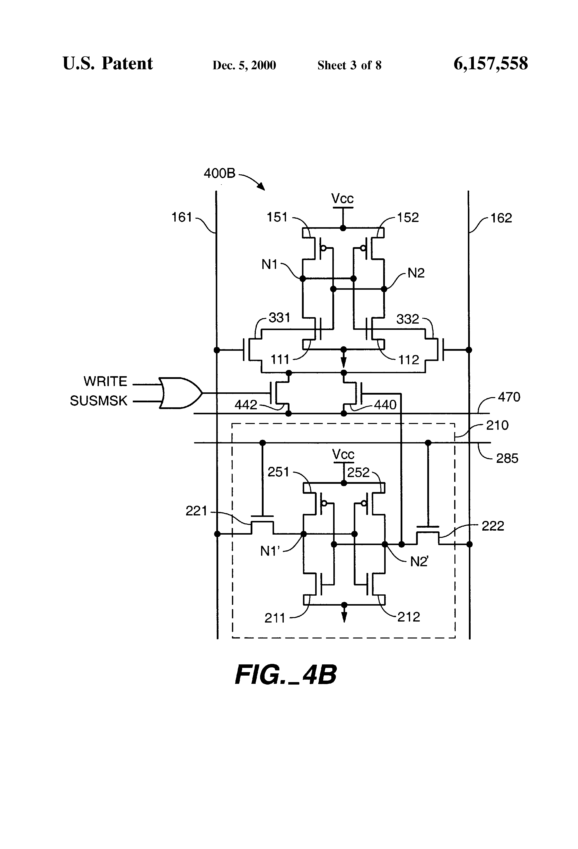
FIG. 4B shows a ternary CAM cell 400B which permits writing even when mask element 210 indicates masking and permits temporary suspension of local masking. CAM cell 400B includes the elements of CAM cell 400 connected as described above in regard to FIG. 4A, but CAM cell 400B further includes a transistor 442 connected in parallel with transistor 440 between word/match line 470 and transistors 331 and 332. The gate of transistor 442 receives a signal WRITE or a signal SUSMSK that is asserted during a write operation. Signal WRITE can be generated on a global basis for all CAM cells 400B in an array or for a selected row of CAM cells 400B when the gate of transistor 442 is connected to a write word line (not shown). When signal WRITE is asserted high, transistor 442 turns on, and a low voltage on word/match line 470 transfers through transistor 442 and transistor 331 or 332 to node N1 or N2 for a write operation, regardless of the state of mask element 210. Accordingly, the state of mask element 210 does not need to be changed for a write operation performed on CAM cell 400B.
Another feature of CAM cell 400B is the ability to temporarily turn off local masking without changing the state of mask element 210. Signal SUSMSK being asserted (high) during a search operation turns on transistor 442 and connects transistors 331 and 332 to match/word line 370. Accordingly when signal SUSMSK is asserted, CAM cell 400B operates in the same manner as binary CAM cell 300 of FIG. 3. With transistor 442 off (signal SUSMSK deasserted), CAM cell 400B operates in the same manner as ternary CAM cell 400. Signal SUSMSK can be generated on a global basis for an entire array or on a row-by-row basis to suspend masking only in one or more selected rows.
A concern for ternary CAM cells 400 and 400B is the power-up state of mask element 210. Typically, with a bi-stable storage element such as mask element 210, the power-up state of the storage element is undetermined. A mask operation can set mask element 210 in a known state. Alternatively, transistors 211, 212, 251, and 252 can be given different dimensions to create a preferred power-up state to which mask element 210 settles. For example, if cell 400 or 400B needs to be in the "no masking" state when power up occurs, node N2' needs to go to "high", and node N1' needs to go to "low". This can be achieved by skewing the dimensions of cross-coupled transistors 211, 212, 251, and 252 so that the ratio of the channel width to channel length for transistor 252 is greater than the ratio of the channel width to channel length for transistor 251, and the ratio of the channel width to channel length for transistor 211 is greater than the ratio of the channel width to channel length for transistor 212.
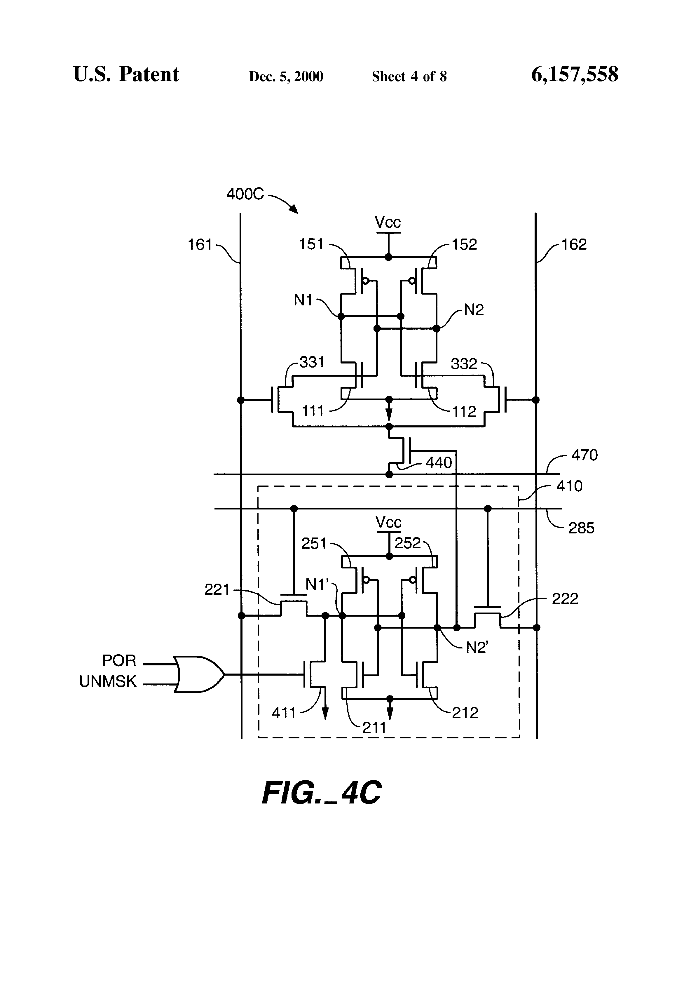
FIG. 4C shows a ternary CAM cell 400C having a mask element 410 that powers up in a known state. CAM cell 400C contains the same elements as CAM cell 400 of FIG. 4A, but CAM cell 400C additionally includes an N-channel transistor 411 coupled to pull-down node N1' in mask element 410, during start up. In particular, transistor 411 connects between node N1' and ground and has a gate which receives a power-on-reset signal POR. When a circuit containing CAM cell 400C is turned on or reset, signal POR is briefly asserted causing transistor 411 to pull node N1' down to the low voltage state so that CAM cell 400C is in the "no masking" state. Other connections of transistor 411 (e.g., to node N1' or N2' and to ground or supply voltage Vcc) can be used to ensure either the "no masking" state or the "masking" state. Additionally, mask element 410 of CAM cell 400C can replace mask element 210 in CAM cell 400B of FIG. 4B if both a known power up state and the ability to ignore local masking are required.
Another advantage of having pull-down transistor 411 or another device in mask element 410 is ability to easily set mask element 410 in the "no masking" state during operation of CAM cell 400C. When a signal UNMSK is asserted (high), transistor 411 pulls down node N1' thereby setting mask element 410 in the "no masking" state. Signal UNMSK can be generated on a global basis to remove all local masking in an array of CAM cells 400C or on a row-by-row basis to turn off local masking only in one or more selected rows of a CAM array.
FIG. 5 shows a CAM 500 including an array 510 of the CAM cells 300 of FIG. 3. Array 510 is simplified for ease of illustration. An actual CAM array includes hundreds or thousands of rows with hundreds of CAM cells 300 per row. CAM 500 includes a word/match line control circuit 520 coupled to word/match lines 370, a bit line control circuit 530 coupled to bit lines 161 and 162, sense amplifiers 540 coupled to word/match lines 370, and a priority encoder 550 coupled to sense amplifiers 540. Word/line control circuit 520 includes selection and bias circuits. The selection circuit is an address decoder that selects a word/match line 370 that an address signal ADRIN identifies. The bias circuits bias selected and unselected word/match lines 370 for write and search operations. Bit line control circuit 530 biases pairs of bit lines 161 and 162 according to associated bits of an input signal DATA-- IN. Sense amplifiers 540 sense word/match lines 370 during a search and generate match signals to indicate which of the rows of array 510 store CAM words matching an input value. Priority encoder 550 converts the match signals into an output signal ADROUT corresponding to any CAM words that match the input signal.
For a writing of a word to array 510, word/match line control circuit 520 receives an address signal ADRIN that identifies a word/match line and its associated row of CAM cells 300 in array 510 for the write, and bit line control circuit 530 receives a data signal DATA-- IN indicating a word to be written to the selected row of CAM cells 300. Control circuit 520 grounds the selected word/match line 370 and biases the unselected word/match lines 370 at supply voltage Vcc. Bit line control circuit 530 applies to each pair of bit lines 161 and 162, complementary signals representing the bit from signal DATA-- IN that is being written in a CAM cell 300 that is connected to the bit lines 161 and 162 and in the selected row. Since the unselected word/match lines 370 are at supply voltage Vcc and the selected word/match line 370 is grounded, the signals on bit lines 161 and 162 only change the states of CAM cells 300 in the selected row.
For a search, signal DATA-- IN to bit line control circuit 530 indicates a search value for simultaneous comparison to the CAM words stored in array 500. Word/match line control circuit 520 charges all of the word/match lines 370 to supply voltage Vcc, and bit line control circuit 530 applies to each pair of bit lines 161 and 162, complementary signals representing the associated bit from signal DATA-- IN. The complementary signals that control circuit 530 uses to represent a bit value during the search are opposite to the complementary signals that control circuit 530 uses to represent the bit value during a write operation. Each sense amplifier 540 senses whether CAM cells 300 discharge the word/match line 370 associated with the sense amplifier, and "match" signals from the sense amplifiers 540 to priority encoder 550 indicate whether the associated CAM words match the search value. Priority encoder 550 interprets the match signals and generates an output signal (or address) ADROUT corresponding to a CAM word that matches the search value. For routing applications of CAM 500, signal ADROUT can be value selected from a look-up table included in priority encoder 550. When multiple CAM words match the search value, priority encoder 550 outputs signal ADROUT corresponding to the CAM words according to a priority order for the CAM words. The priority order, for example, may be based on the row addresses for the CAM words, the order in which CAM words are physically mapped into CAM 500, or which CAM word priority encoder 550 was last identified as a match. Priority encoders such as priority encoder 550 are well known for CAMs.
FIG. 6 is a block diagram of a CAM 600 including an array 610 of ternary CAM cells 400 of FIG. 4A. Array 610 is simplified for illustration but would normally contain hundreds or thousands of rows and columns of CAM cells 400. Coupled to array 610 are a word/match line control circuit 520, a bit-by-bit local masking control circuit 620, a bit line control circuit 530, and sense amplifiers 540. Priority encoder 550 connects to and receives match signals from sense amplifiers 540 as described above in regard to FIG. 5. CAM 600 differs from CAM 500 in that array 610 and ternary CAM cells 400 have word lines 285 for masking operations and control circuit 620 controls masking word lines for write, search, and bit-by-bit local masking operations.
For a masking operation, an address signal MA identifies a selected row of array 610 for which the masking is to be changed, and input signal DATA-- IN indicates which CAM cells 400 (or CAM bits) in the selected row, are to have masking enabled or disabled. For the masking operation, masking control circuit 620 biases the selected mask word line 285 to supply voltage Vcc and grounds all unselected mask word lines 285, and word/match line control circuit 520 biases all word/match lines 470 to supply voltage Vcc. Bit line control circuit 530 biases each pair of bit lines 161 and 162 with complementary signals indicating the state desired for local masking in a CAM cell 400 that is in the selected row and coupled to the bit lines.
For a write operation to a CAM word, address signal ADRIN selects a row for the write operation, and signal DATA-- IN indicates the word to be written. For the write operation to work, none of the CAM cells 400 corresponding to the select CAM can have local masking. An optional register (not shown), which includes one bit of storage for each CAM word in array 610, can be set to indicate which CAM words or rows include at least one cell with a locally masked bit. If there is no local masking in a particular row, a write operation can proceed without an initial masking operation. Otherwise, CAM 600 performs a masking operation to remove any masking of CAM cells 400 in the selected row. After the unmasking, control circuit 520 grounds the selected word/match line 470 and biases the unselected word/match lines 470 to near supply voltage Vcc, and mask control circuit 620 grounds all mask word lines 285 so that writing of a CAM word does not affect the mask elements 210. Bit line control circuit 530 then biases each pair of bit lines 161 and 162 with complementary signals indicating a bit to be written in a CAM cell 400 that is in the selected row and coupled to the bit lines.
For a search, control circuit 620 grounds all mask word lines 285, and control circuit 520 charges all word/match lines 470 to near supply voltage Vcc. Next, bit line control circuit 530 biases bit lines 161 and 162 according to the input data that signal DATA-- IN represents. Sense amplifiers 540 generate match signals according to which of row(s) of array 610 include CAM cell(s) 400 that detectably pull down their associated match/word line(s) 470, and priority encoder 550 generates output signal ADROUT from the match signal(s) as described above.
FIG. 7 shows a CAM 700 in accordance to another embodiment of the invention. CAM 700 includes an array 710 of ternary CAM cells 715. Each ternary CAM cell 715 differs from the ternary CAM cell 400 of FIG. 4A in that pass transistors 221 and 222 for the mask element connect to bit lines 761 and 762 which are separate from the bit lines 161 and 162 used for write and search operations. Accordingly, write and search operation use a set of bit lines 161 and 162, and local masking operations use a different set of bit lines 761 and 762. In CAM 700, bit line control circuit 530 controls bit lines 161 and 162 for write and search operations, and a local masking bit line control circuit 730 controls mask bit lines 761 and 762 for mask operations. This provides greater flexibility in design of control circuits 520 and 620 since word/line control circuit 520 does not need to bias word/match lines 470 during a masking operation, and mask word line control circuit 620 does not is need to bias mask word lines 285 for write or search operations. Further, higher performance can be achieved because CAM 700 can conduct a masking operation simultaneously with a write operation or a search.
Although much of the above disclosure concentrated CAM cell architectures that reduce transistor count using strategically placed transistors with control terminals coupled to bit lines. Other aspects of the invention can be employed in CAM cells having more traditional storage elements. For example, the ability to temporarily turn off local masking is also desirable in conventional ternary CAM cells such as CAM cell 200 of FIG. 2. FIG. 8 illustrates a memory cell 800 having a storage element including transistors 111, 112, 121, 122, 131, 132, 141, 142, 151, and 152 as described above in regard to FIG. 2, except that transistors 141 and 142 connect to match line 170 through N- channel transistors 442 and 840. Mask element 410 couples to the gate of transistor 840 and controls whether or not transistor 840 conducts. In particular, when node N2' is "high", transistor 840 conducts, and CAM cell 800 is unmasked. When node N2' is low, transistor 840 does not conduct, and CAM cell 800 is locally masked (i.e., in the "don't care state"). However, even when the state of mask element masks CAM cell 800, transistor 442 temporarily suspends or supersedes the local masking when signal WRITE causes transistor 442 to conduct.
CAM cell 800 also includes the feature of using mask element 410 which includes circuitry (transistor 411) for ensuring that mask element 410 powers up with a known masking state. Operation of mask element 410 is described above in regard to FIG. 4C.
Although the invention has been described with reference to particular embodiments, the description is only an example of the invention's application and should not be taken as a limitation. In particular, even though much of preceding discussion specified specific transistor types, alternative embodiments of are not limited to the specific types disclosed. Various other adaptations and combinations of features of the embodiments disclosed are within the scope of the invention as defined by the following claims.