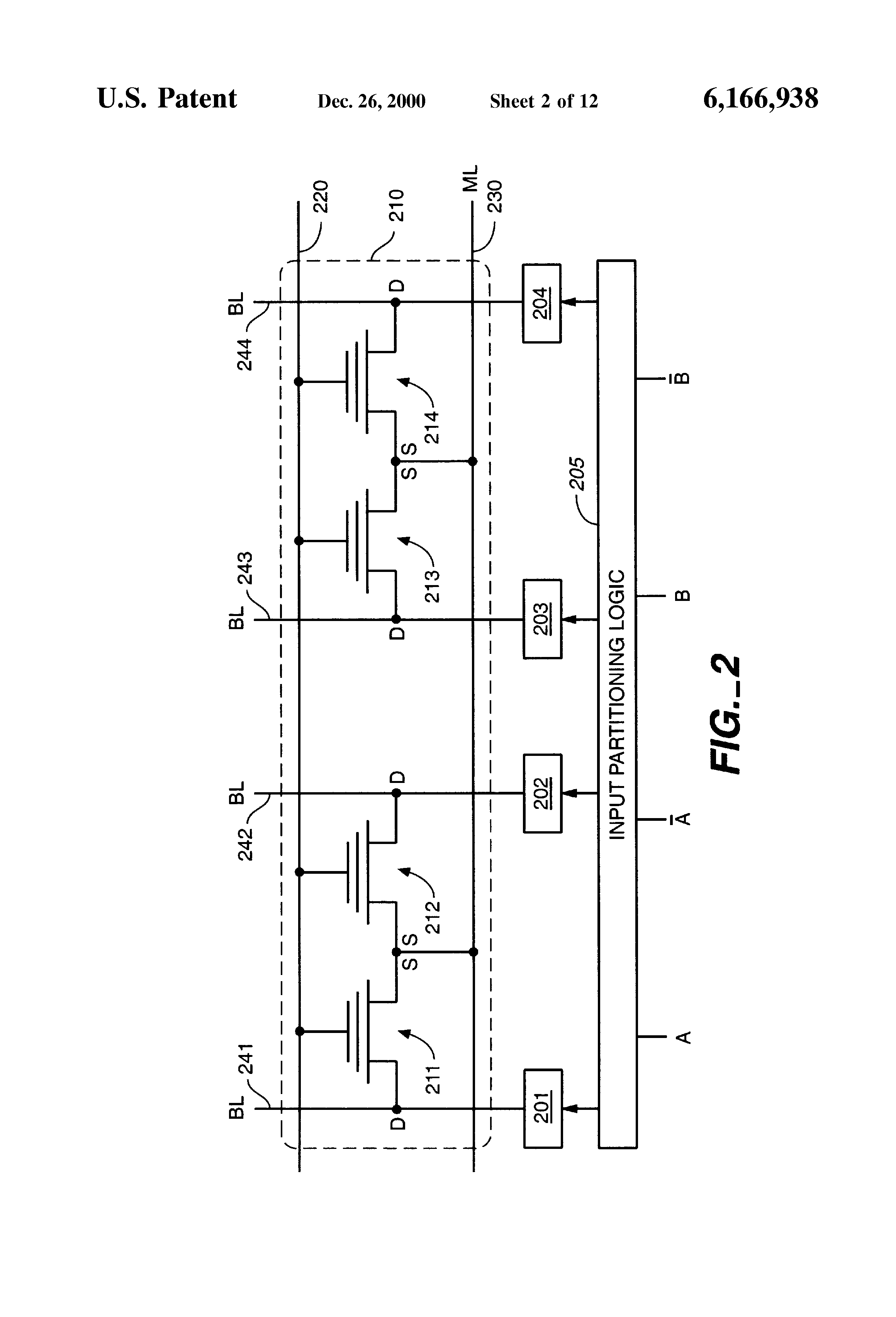
FIG. 2 shows a 4-T non-volatile Flash CAM cell 210 with tri-state bit-line drivers 201-204 and input partitioning logic 205 in accordance with an embodiment of the invention. CAM cell 210 is formed from a pair of two-transistor (2-T) Flash CAM cells, such as described in commonly-owned U.S. pat. appl. Ser. No. 09/293,134, entitled "Non-Volatile Content Addressable Memory", filed Apr. 16, 1999, bearing attorney Docket No. M-7323 US, which is incorporated by reference in its entirety. 4-T CAM cell 210 includes four floating-gate transistors 211-214 coupled to a word-line 220, a match-line 230, and four respective bit-lines 241-244. Floating-gate transistors 211-214 are single-transistor Flash memory cells of the kind used in conventional Flash memory, but alternative embodiments of the invention can replace transistors 211-214 with any type of non-volatile memory cells having a control gate, a source terminal, and a drain terminal available for connection as shown in FIG. 2. In CAM cell 210, word-line 220 couples to the control gates of transistors 211-214. Match-line 230 couples to the sources of transistors 211-214, and bit-lines 241-244 couple to respective drains of transistors 211-214. CAM cell 210 can store a pair of data bits and compare the stored bits to a pair of input bits that signals on bit-lines 241-244 represent.
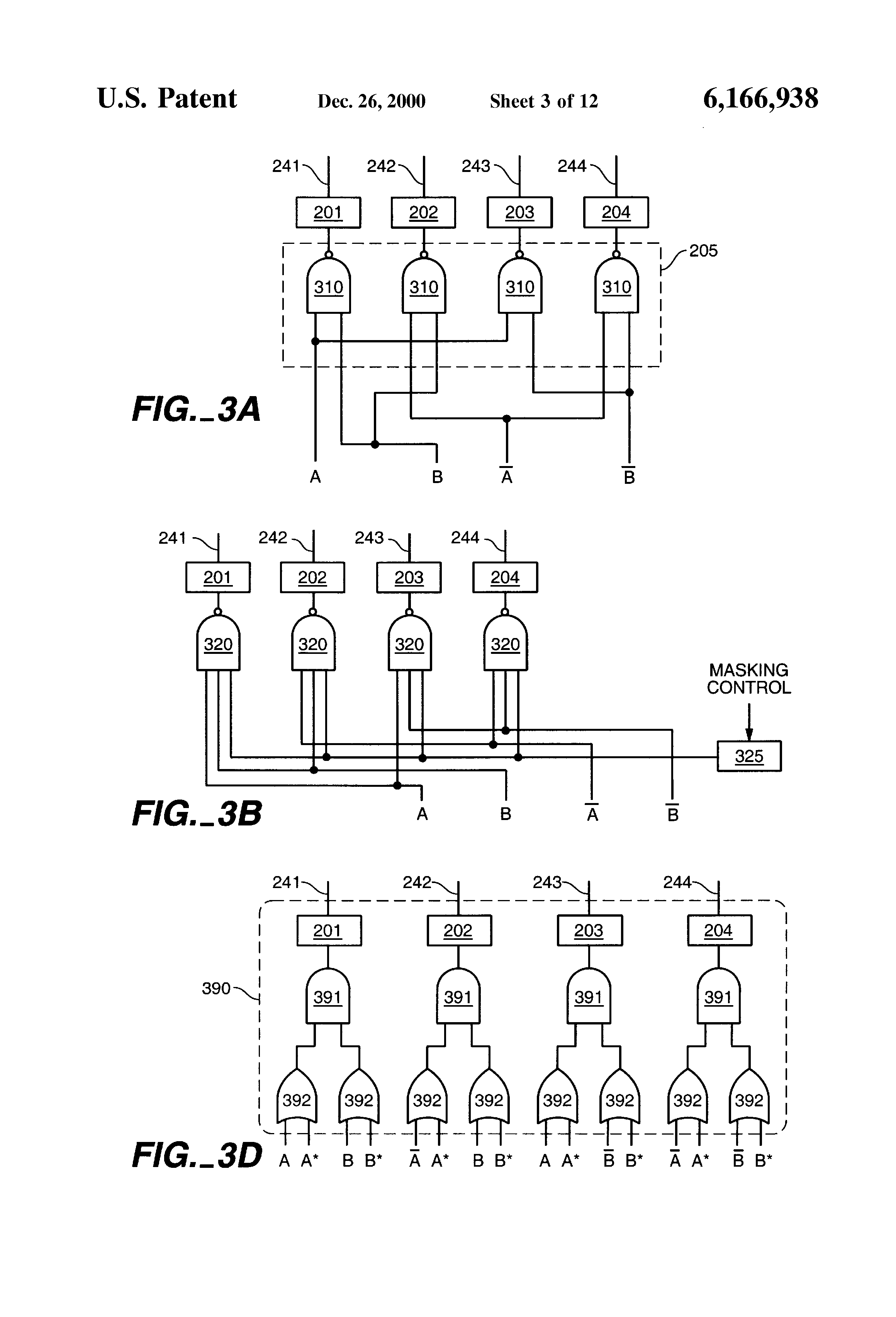
Input partitioning logic 205, according to one embodiment shown in FIG. 3A, includes four two-input NAND gates 310 coupled to bit-line drivers 201-204, which are coupled to bit-lines 241-244. Each of four distinct pairs of input signals A and B and their complements are input to NAND gates 310. Depending on the value of signals A and B, a unique set of signals are applied to bit-line drivers (BLDs) 201-204, as shown in Table 2.
As seen from Table 2, the input to one distinct bit-line driver is low for each of the four AB bit-pair combinations, thereby allowing transistors attached to a particular bit-line driver to be programmed or searched corresponding to one of the four bit-pair combinations. Thus, according to one convention, transistor 214 (attached to BLD 204) being programmed indicates 00 stored in CAM cell 210, transistor 212 (attached to BLD 202) being programmed indicates 01 stored in CAM cell 210, transistor 213 (attached to BLD 203) being programmed indicates 10 stored in CAM cell 210, and transistor 211 (attached to BLD 201) being programmed indicates 11 stored in CAM cell 210.
The write operation programs CAM cell 210 to store a pair of data bits, as mentioned above. For each CAM cell 210, floating-gate transistors 211-214 are individually programmable. The storage convention described above writes a 00 in CAM cell 210 by programming the threshold voltage of transistor 214 to a high threshold voltage state (Vt>Vcc) while transistors 211-213 remain in the low (or erased) threshold voltage state. Programming the threshold voltage of transistor 212 to the high threshold voltage state while transistors 211, 213, and 214 remain in the low threshold voltage state writes a 01 in CAM cell 210. Programming the threshold voltage of transistor 213 to the high threshold voltage state while transistors 211, 212, and 214 remain in the low threshold voltage state writes a 10 in CAM cell 210. Finally, 11 is stored in CAM cell 210 by programming the threshold voltage of transistor 211 to the high threshold voltage state while transistors 212-214 remain in the erased state. Thus, 4-T CAM cell 210 can be programmed to store one of four bit-pairs 00, 01, 10, and 11 by programming one of the four transistors 211-214 to a high threshold voltage state, while the remaining three transistors remain in a low threshold voltage state.
Global masking on bit-pairs (i.e., along the same two bit-lines for all words in an array) or a more "selective" masking in which bit-pairs along the same two bit-lines and also along selected word-lines can also be used with the present invention. FIG. 3B shows masking with the NAND partitioning logic of FIG. 3A. Depending on a masking control signal, a masking register 325 applies either a "high" signal (no masking) or a "low" signal (masking) to each of four 3-input NAND gates 320. Without masking, the high signal from register 325 does not affect the output of NAND gates 320, i.e., the output is only dependent on the logic states of inputs A and B. However, with masking, the low signal from register 325 forces the output of NAND gates 320 to be high, regardless of the state of inputs A and B. Consequently, with masking, transistors 211-214 of different words connected to the same bit-lines 241-244, which are each programmed to either a high or low threshold voltage state, can effectively represent a bit-pair designated by "XX" ("don't care" state for the bit-pair).
Masking where transistors 211-214 are programmed to the high threshold voltage state enables a search operation to indicate a "match" regardless of the search inputs A and B. This also allows a more selective masking in that all the transistors coupled to the associated bit-lines do not have to be masked, only those that have also been selected by word-lines 220 at the programming voltage. Note that if masking is only utilized during programming operations (i.e., register 325 applies a low signal only during programming), floating-gate transistors 211-214 can only be programmed each to the high threshold voltage state, as will be discussed below in conjunction with the search operations, which effectively programs the bit-pair of a selected word to a "don't care" state. In this case, "unmask" operation requires erasing all four floating-gate transistors 211-214 and then writing the required data back into them before a search.
For programming a selected floating-gate transistor 211-214 in CAM cell 210, a high voltage Vpp (e.g., about 8 to 12 volts) is applied to word-line 220, and 0 volt or ground is applied to match-line 230. An associated one of bit-line drivers 201-204 applies a programming voltage Vw (e.g., about 5 to 6 volts) to the bit-line 241-244 coupled to the selected floating-gate transistor 211-214. Bit-lines 241-244 that are coupled to unselected transistors remain grounded or float. The power supply for bit-line drivers 201-204 can switch between Vcc during a search operation to Vw during a program or write operation. The combination of these voltages on the selected floating-gate transistor 211-214 causes channel hot electron (CHE) injection that programs the selected transistor to the high threshold voltage state where the threshold voltage is higher than supply voltage Vcc.
Table 3 below lists programming voltages Vw applied by bit-line drivers 201-204 to respective bit-lines 241-244 for each bit-pair combination to program or write data values to an attached one of transistors 211-214 corresponding to the bit-pair combination. A "don't care" state, designated by AB=XX, is also included in Table 3.
Prior to programming selected transistors, CAM cell 210 is erased by erasing floating-gate transistors 211-214. A negative-gate erase operation for CAM cell 210 applies a negative voltage (e.g., -8 to -10 volts) to word-line 220 (i.e., to the control gates) and applies a positive voltage (e.g., 5 to 7 volts) to match-line 230 (i.e., to the sources). The erase operation can employ alternative erases methods such as a grounded-gate erase or channel erase. Commonly-owned U.S. pat. appl. Ser. No. UNKNOWN, entitled "Non-Volatile Memories with Improved Endurance and Extended Lifetime", filed Apr. 16, 1999, bearing attorney Docket No. M-7357 US, describes suitable erase methods which can further improve Flash memory cell endurance and is hereby incorporated by reference in its entirety. The combination of the control gate and source voltages causes Fowler-Nordheim (FN) tunneling in transistors 211-214. The FN tunneling removes electrons from the floating gates and lowers threshold voltages of transistors 211-214. The erase operation places transistors 211-214 in a low threshold voltage state, for example, where the threshold voltage Vt is less than about 1 volt when supply voltage Vcc is about 3 volts, or less than about 0.5 volts when supply voltage Vcc is about 1.8 volts.
For a search, word-line 220 and match-line 230 are charged to near supply voltage Vcc, and complementary binary signals A and A and B and B are applied in various logic combinations to bit-lines 241-244. The convention for representing a bit-pair on bit-lines 241-244 during a search is opposite to the convention described above for storing bit-pairs in CAM cell 210. For example, if transistor 212 is in the high threshold voltage state and transistors 211, 213, and 214 are in the low threshold voltage or erased state to store a 01, ground or 0 volt is applied to bit-line 242 attached to transistor 212, and supply voltage Vcc is applied to bit- lines 241, 243, and 244 attached to respective transistors 211, 213, and 214 to represent a search for bit-pair 01. Different conventions could be used for both the data storage and the search signals. Because word-line 220 during a search is at supply voltage Vcc, none of the transistors 211-214 that are in the high threshold voltage state (which has a threshold voltage higher than Vcc) conduct. Transistors 211-214 in the low threshold voltage state conduct only if the bit-line 241-244 attached to the corresponding transistor is at 0 volt or grounded.
Referring back to FIG. 3B, whereas programming transistors 211-214 allows "selective masking", as discussed above, global masking for each bit-pair is also possible during search operations. Global masking allows each of the four transistors 211-214 in CAM cell 210 to be either in the high or low threshold voltage state. When global masking is utilized during a search operation, register 325 applies a low signal to NAND gates 320, which causes bit-line drivers 201-204 to apply high signals to bit-lines 241-244. Therefore, none of transistors 211-214 conduct, regardless of whether input A or B is at a high or low state. Consequently, a match of all the CAM cells along the same bit-lines always results with global masking regardless of the programmed state of transistors 211-214. To unmask the CAM cell during a search, mask register 325 can later apply a "high" signal to each of the four three-input NAND gates 320 to unmask and resume the search for matches with input bit pairs. However, if selective masking is utilized during a programming operation and no masking is used during a search operation, floating-gate transistors 111-114 of a selected word are each programmed to the high threshold voltage state. This is the "don't care" state because no current can flow through floating-gate transistors 211-214 regardless of the logic state of bit-lines 241-244 during a search.
Table 4 indicates the possible combinations of stored and input search bits and some of the parameters of CAM cell 210 during a search.
A match for a CAM cell 210 occurs when none of the four transistors 211-214 conduct, thereby preventing discharge of the voltage on the match-line 230.
As seen from a comparison between Table 1 and Table 4, only one out of four transistors in 4-T CAM cell 210 is programmed using the NAND partitioning logic described above, as compared with two out of the four transistors using conventional methods, and searching the data stored in 4-T CAM cell 210 requires only two transitions from Vcc to ground or ground to Vcc, instead of up to four such transitions with conventional methods. Lower programming and switching requirements result in a CAM array using less AC power (up to 50% less). Furthermore, because only one (instead of two) out of four transistors in each 4-T CAM cell is programmed, less programming current is needed and CAM cell endurance effectively improves.
Although the above has been described with a NAND partitioning logic, other types of partitioning logic can also be used to achieve the benefits of the present invention. For example, Table 5 shows the signals applied to bit-line drivers 201-204 using an AND partitioning logic. The voltage levels for programming and search operations are the same as described above. However, with AND partitioning, three out of the four transistors in the CAM cell need to be programmed to a "high" state, while the remaining transistor remains in the "low" or erased state because the polarities of the search signals are opposite to those shown in Table 2 for NAND input partitioning.
In other embodiments, partitioning logic using an OR function is shown in Table 6. In this situation, programming transistor 211 associated with BLD 201 to a high threshold voltage state while leaving transistors 212-214 in an erased or low threshold voltage state corresponds to a stored bit-pair 00. Similarly, the stored bit-pair 01 corresponds to only transistor 213 associated with BLD 203 being programmed to the high threshold voltage state, the stored bit-pair 10 corresponds to only transistor 212 associated with BLD 202 being programmed to the high threshold voltage state, and the stored bit-pair 11 corresponds to only transistor 214 associated with BLD 204 being programmed to the high threshold voltage state.
Table 7 shows the possible combinations of stored and input search bits and some of the parameters of CAM cell 210 during a search using OR partitioning logic.
As seen from Table 7, only one transistor is programmed for each of the four bit-pair combinations, and only two transitions from Vcc to ground or ground to Vcc occur on the bit-lines during searches, thereby providing the same advantages as with the NAND partitioning logic described above.
Table 8 shows the signals applied to bit-line drivers 201-204 using a NOR partitioning logic. The voltage levels for programming and search operations are the same as described above. Similar to the AND partitioning, however, three out of the four transistors in the CAM cell need to be programmed to a "high" state, while the remaining transistor remains in the "low" or erased state when using OR partitioning.
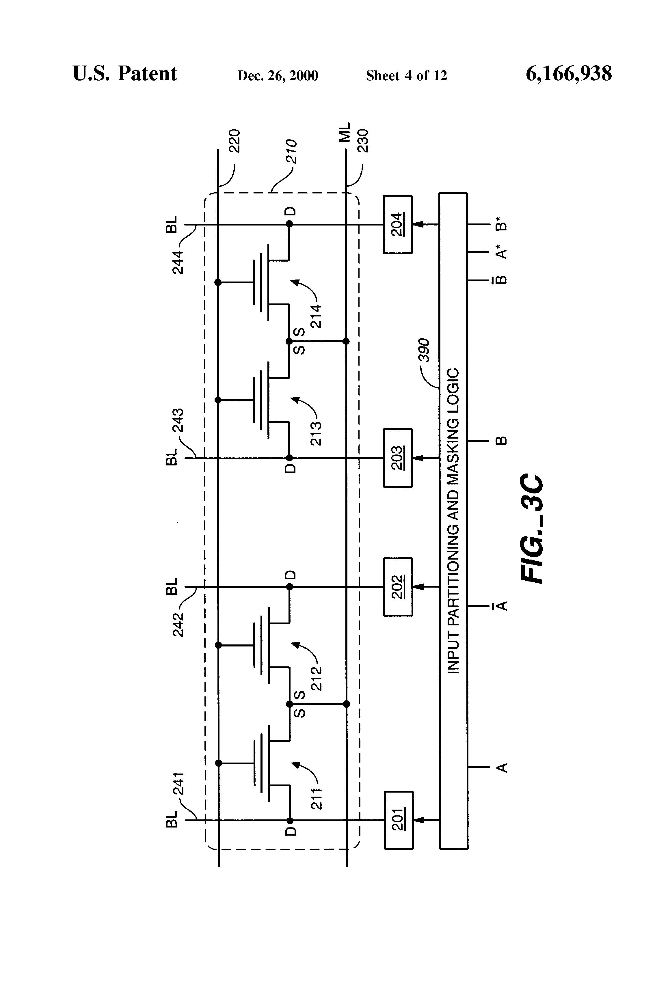
In addition to the various logical functions usable with input partitioning logic 205 and the per-bit pair global masking, bit-by-bit global masking can be incorporated into input partitioning logic 205 in other embodiments of the invention. FIG. 3C shows an input partitioning and masking logic 390 coupled to 4-T Flash CAM cell 210. Logic 390 is similar to logic 205, as described above, except that masking bits A* and B* are also input to logic 390 in addition to the input bits A and B and their complements. The masking bits A* and B* can be selected from a masking register (not shown) when a masking is desired.
FIG. 3D shows input partitioning and masking logic 390 using AND partitioning logic according to one embodiment. Logic 390 includes four two-input AND gates 391 having outputs coupled to drivers 201-204 and inputs coupled to two two-input OR gates 392. Each pair of OR gates 392 has one input each corresponding to an original pair of input bits A, A, B, and B. The other input of each of the pair of OR gates 392 is masking bit A* and masking bit B*. When masking bit A* is high, bits A and A are masked, and when masking bit B* is high, bits B and B are masked. By selecting masking bit A* or masking bit B* high during a write operation, transistors 211 and 212 can be programmed high for a "don't care" state or transistors 213 and 214 can be programmed high for a "don't care state". Thus, bit-by-bit global masking of the CAM cell is possible. If both masking bits A* and B* are high during a write operation, all four transistors 211-214 are programmed high, resulting in a "don't care" state for the bit-pair (i.e., per-bit-pair masking).
Input partitioning logic 205 can be applied to various CAM architectures, such as those described in commonly-owned U.S. pat. app. Ser. No. UNKNOWN, entitled "Non-Volatile Content Addressable Memory", incorporated by reference above. FIG. 4 shows one such Flash CAM 400 which includes an array 450 of substantially identical 4-T non-volatile CAM cells 210. Flash CAM 400 also includes a row control block 460 that couples to word-lines 220 and match-lines 230, sense amplifier blocks 480 that couple to match-lines 230, and bit-line drivers 201-204 that couple to bit-lines 241-244, respectively. Input partitioning logic 205 is coupled between bit-line drivers 201-204 and input signals A, A, B, and B. Each of N input partitioning logic 205 is associated with one of N 4-T CAM cells 210 and one of N sets of input signals Ai, Ai , Bi, Bi . Input signals Ai, Ai , Bi, and Bi are selected from a selection circuit (not shown) depending on the bit-pair to be stored or searched in a corresponding CAM cell 210. Row control block 460 controls the voltages on word-lines 220 and match-lines 230 for erase, program, read, and search operations. Row control block 460 typically includes an address decoder (not shown) that selects a row of CAM cells 210 according to an address signal ADRIN identifying a row for a write or read operation. Bias circuits (not shown) in block 460 apply voltages to selected and unselected word-lines 220 and match-lines 230 as required for the different operations.
Sense amplifier blocks 480 sense current or voltage drops on match-lines 230 that identify stored words that do not match an input value. Bit-line drivers 201-204 control the voltages on bit-lines 241-244 for erase, program, search, and read operations. Bit-line drivers 201-204 each include tri-state drivers (not shown), with the output of each of the tri-state drivers coupled to a corresponding bit-line 241-244 in array 450. When the input to a tri-state driver is low, that driver is off and the corresponding bit-line is grounded. When the input to a tri-state driver is high, that driver is on and applies an appropriate program voltage (e.g., Vw) higher than supply voltage Vcc or search voltage (e.g., Vcc) to the corresponding bit-line. The illustrated blocks 460 and 480 can be implemented using circuits and techniques well known for non-volatile memories.
During a search, a match for a CAM word occurs when all of the CAM cells 210 in the row corresponding to the CAM word find a match so that none of the CAM cells 210 discharge the voltage on the match-line 230. A priority encoder 485 interprets the match signals from sense amplifier blocks 480 and generates an output signal ADROUT corresponding to the word in CAM 400 which matches the input value. When multiple CAM words match the input value, priority encoder 485 selects and outputs signal ADROUT corresponding to the CAM word that has the highest priority, followed by the CAM word that has the next highest priority, and so on until the last matching CAM word is identified.
Optional read circuitry 495 can be connected to bit-lines 241-244 for a parallel read operation. Read circuitry 495 includes, for example, bit-line bias circuits and sense amplifiers that couple to bit-lines 241-244. A bit-line bias circuit biases or charges an attached bit-line for reading (e.g., to about 1.5 volts) while block 460 biases a selected word-line 220 to voltage Vcc and grounds match-lines 230 and unselected word-lines 220. The bit-line sense amplifiers in read circuitry 495 sense currents or voltage drops on the attached bit-lines for a fast parallel read-out of a word from CAM 400. The parallel read operation is typically faster and more convenient for testing of CAM 400 and other product or architectural uses.
Further, Flash CAM 400 can include a CAM buffer 490 capable of a fast write operation. In an exemplary embodiment, CAM buffer 490 is a SRAM-based CAM including storage for at least one word. Alternatively, a DRAM-based CAM buffer could be used, but DRAM requires overhead for refresh operations. Such refresh circuitry is typically not warranted for the small amount of storage in CAM buffer 490. In another embodiment, CAM buffer 490 includes non-volatile CAM cells that are pre-erased in anticipation of the initiation of a write operation. In an application of CAM 400 where writing is relatively infrequent, erase operations for non-volatile cells in buffer 490 can be performed in the background of operation of CAM 400. With pre-erased rows, writing to CAM buffer 490 only requires programming of CAM cells, and does not need to wait for the erase operation to complete.
A write operation to CAM 400 temporarily stores an input word in CAM buffer 490 while a row of non-volatile array 450 is erased and subsequently programmed. Writing to CAM buffer 490 is fast when compared to the writing operations for non-volatile CAM array 450 which requires an erase operation prior to programming. With CAM buffer 490 holding a value to be written in array 450, CAM 400 can perform a search while the write operation erases a word in non-volatile array 450. In particular, as mentioned above, biasing bit-lines 241-244 for a search does not disturb an erase operation. Similarly, row control block 460 biases the word-line 220 and match-line 230 of a selected row or rows for the erase operation while biasing word-lines 220 and match-lines 230 for every other row of array 450 for the search. Simultaneously with the search in non-volatile array 450, CAM buffer 490 searches temporarily stored values for a match, and a signal from CAM buffer 490 indicates whether the input value matches a word being written.
Priority encoder 485 accepts match signals from both array 450 (via sense amplifier blocks 480) and CAM buffer 490, which includes a sense amplifier block (not shown). If any row that is not being erased contains a word matching the input value, the associated sense amplifier block 480 signals to priority encoder 485, and priority encoder 485 handles the match signals from sense amplifier blocks 480 in the same manner as described for searches without simultaneous erase operations. Each sense amplifier block 480 that corresponds to a row being erased is disabled or ignored. If CAM buffer 490 signals that the word being written matches the input value, priority encoder 460 sets output signal ADROUT corresponding to the row to which the word is being written. For multiple matches, priority encoder 485 can sequentially output signal ADROUT according to a predetermined order for the CAM words such as according to the binary addressing order.
In FIG. 4, CAM buffer 490 couples to bit-lines 241-244. This connection can be used during a search if the storage convention for the CAM cells of CAM buffer 490 are consistent with the signals on bit-lines 241-244 during a write operation. In other words, CAM buffer 490 has to use the same input partitioning scheme as array 450. However, CAM buffer 490 can be separate from array 450 and include its own write and match circuits. As indicated above, memory 400 is capable of back-to-back write and search operations since array 450 and buffer 490 can perform a search while a row of array 450 is being erased. Similarly, CAM 400 can simultaneously or sequentially erase multiple rows for back-to-back write operations with CAM buffer 490 storing the words to be written to array 450 when the corresponding rows in CAM array are ready for programming.
FIGS. 5-9 show other CAMs that can be used with the input partitioning logic of the present invention. Additional details of the CAMs of FIGS. 5-9 can be found in the above-referenced U.S. Pat. App. "Non-Volatile Content Addressable Memories". FIG. 5 shows a non-volatile CAM 500 that includes an array 550 of CAM cells 510, each CAM cell 510 including a pair of floating-gate transistors 211-214 sharing a common match-line 530. As with CAM 400 of FIG. 4, bit-line drivers 201-204 apply the appropriate voltages to corresponding bit-lines 241-244 based on input partitioning logic 205. Transistors 211-214 connect to a word-line 520 or 525 and bit-lines 241-244. CAM array 550 differs from CAM array 450 of FIG. 4 in that two adjacent rows of CAM cells 510 share a single match-line 530. The sharing of match-lines 530 between two adjacent CAM words can significantly reduce the silicon area required for forming CAM 500 as an integrated circuit, but only half of the rows of CAM cells 510 in array 550 can perform a search at one time. Thus, a search operation in CAM 500 takes two cycles. The search can stop after the first cycle if a match is found. Alternatively, match results from the first cycle of the search can be stored in latches 581. During a second cycle of the search, the states of match-lines 530 indicate whether any odd-numbered row of array 550 contains a match to the input value. The results from both cycles of the search can be applied to priority decoder 585 either directly or through latches 581.
FIG. 6 illustrates a non-volatile CAM 600 that includes an array 650 of CAM cells 610 having split word-lines. Each CAM cell 610 includes a pair of floating-gate transistors 611 and 612 and a pair of floating-gate transistors 613 and 614 which have sources coupled to the same match-line 230. The drains of transistors 611-614 respectively couple to bit-lines 641-644, and the control gates of transistors 611 and 613 and of transistors 612 and 614 couple to respective word- lines 621 and 622. Appropriate voltages are applied to bit-lines 641-644 based on signals provided to bit-line drivers 201-204 from input partitioning logic 205. In operation, a row control block 660 biases word- lines 621 and 622 in a row of CAM cells 610 to the same voltage so that word- lines 621 and 622 effectively operate as a single word-line that is split and coupled to control gates of floating-gate transistors in adjacent rows. Since transistors in adjacent rows, which share a match-line 230, are associated with the same CAM word, a single cycle search is sufficient for CAM 600. Furthermore, since the match-line is shared between two adjacent rows of CAM cells, the silicon or layout overhead is minimized.
FIG. 7 shows a CAM 700 including an array 750 of CAM cells 710 with shared-floating-gate (SFG) devices 711-714, as described in above-referenced U.S. Pat. App. "Non-Volatile Content Addressable Memories". CAM cell 710 includes four SFG devices 711-714. Each SFG device 711-714 includes a pair of floating-gate transistors which have floating gates and sources connected or coupled together. The sources of each transistor connect to a match-line 730, and the control gates of each transistor connect to a word-line 720. The drains of one transistor in each SFG device 711-714 couple to respective bit (or search)-lines 741-744, and the drains of the other transistor in each SFG device 711-714 couple to respective program-lines 745-748. A column control block 770 is coupled between input partitioning logic 205 and bit-lines 741-744 and program-lines 745-748. Column control block 770 includes program or write circuits, column decoders, and tri-state drivers for selecting and applying the appropriate voltages to bit-lines 741-744 for searches and program-lines 745-748 for programming. CAM 700 also includes row control block 460 which controls biasing of word-lines 720 and match-lines 730, sense amplifier blocks 480 coupled to match-lines 730, CAM buffer 490, read circuits 495, and priority encoder 485 which couples to sense amplifier blocks 480 and CAM buffer 490. Because SFG CAM cells 711-714 have separate bit (or search)-lines 741-744 and program-lines 745-748, CAM 700 containing an array of SFG CAM cells 710 can perform a search operation simultaneously with an erase and/or a programming operation. An array of SFG CAM cells with the architecture described herein can also use a CAM buffer to permit immediate back-to-back write and search operations without delays for either an erase operation or a delay for a programming operation.
FIG. 8 shows a non-volatile CAM 800 including an array 850 of dual CAM cells 810. Array 850 is structurally the same as array 550 of FIG. 5, but each CAM cell 810 contains two 4-T CAM cells 510 of array 550. Thus, each CAM cell 810 is an effective 8-T CAM cell that couples to associated bit-lines 241-244, associated word- lines 820 and 825, and a match-line 830. In each CAM cell 810, a first four of floating-gate transistors 811-814 have control gates coupled to word-line 820 and sources coupled to match-line 830. Respective drains of floating-gate transistors 811-814 connect to respective bit-lines 241-244. A second four of floating-gate transistors 815-818 have control gates coupled to word-line 825 and sources coupled to match-line 830. Respective drains of floating-gate transistors 815-818 connect to respective bit-lines 241-244. Input partitioning logic 205 and bit-line drivers 201-204 couple to bit-lines 241-244, respectively. Similar to other described CAMs above, a row control block 860, read circuit 895, and buffer 890 are connected to array 850.
CAM 800 allows selective masking for a single CAM word, multiple CAM words, or all CAM words in array 850, and the masking implemented for one CAM word can be different from the masking for another CAM word. In particular, a mask select register (not shown) connected to row control block 860 has one mask register bit per CAM word. During a search operation, each mask register bit controls whether row control block 860 applies supply voltage Vcc to word line 820 or 825 in the row of array 850 that corresponds to the bit. Thus, each bit in a CAM word is individually maskable by appropriate programming of the transistors 815-818 in the CAM cells 810 associated with the bit. Masking of a bit does not destroy the original value in CAM array 850 because transistors 811-814 remain in threshold voltage states that indicate the original bit. Masking one bit does not affect other bits on the same word line, which may or may not need masking. An array of dual CAM cells with the architecture described herein can also use a volatile CAM buffer to permit simultaneous erase and searches.
FIG. 9 shows a non-volatile CAM 900 including an array 950 of non-volatile dual CAM cells 910. Each dual CAM cell 910 is an 8-T CAM cell including floating-gate transistors 911-918. Each transistor 911-918 has a drain coupled to a shared drain-line 930. Transistors 911-914 have sources coupled to a word/match-line 921, and transistors 915-918 have sources coupled to a word/match-line 922. Control gates of transistors 911 and 915 couple to bit-line 141, control gates of transistors 912 and 916 couple to bit-line 142, control gates of transistors 913 and 917 couple to bit-line 143, and control gates of transistors 914 and 918 couple to bit-line 144. With these connections, transistors 911-914 form a first CAM element having the same structure as that of the conventional 4-T Flash CAM cell in FIG. 1B, except that the roles of the source and drains of the transistors are reversed. Similarly, transistors 915-918 form a second CAM element having the same structure as the first CAM element. Input partitioning logic 205 couples to tri-state drivers 201-204, which apply the appropriate voltages to bit-lines 141-144, respectively.
A row control block 960 selects desired word/match- lines 921 and 922 based on signal ADRIN and applies proper voltages for the desired operation. Sense amplifiers 981 and 982 sense which word/match- lines 921 and 922, respectively, couple to conductive transistors. Without masking, priority encoder 985 uses signals from sense amplifiers 981 to generate the output signal ADROUT identifying a matching CAM word. For a search with masking, priority encoder 985 uses signals from sense amplifiers 982 to generate output signal ADROUT. Selection of sense amplifier 981 or 982 and match- line 921 or 922 for a search can be on a row-by-row (or CAM word-by-CAM word) basis. In particular, a mask register includes one mask register bit (MRB) 996 per CAM word and applies each bit 996 to a corresponding 2:1 multiplexer 984 as a select signal. Accordingly, the match signals to priority encoder 985 indicate matches with programmable combination of matches with masked and unmasked CAM words.
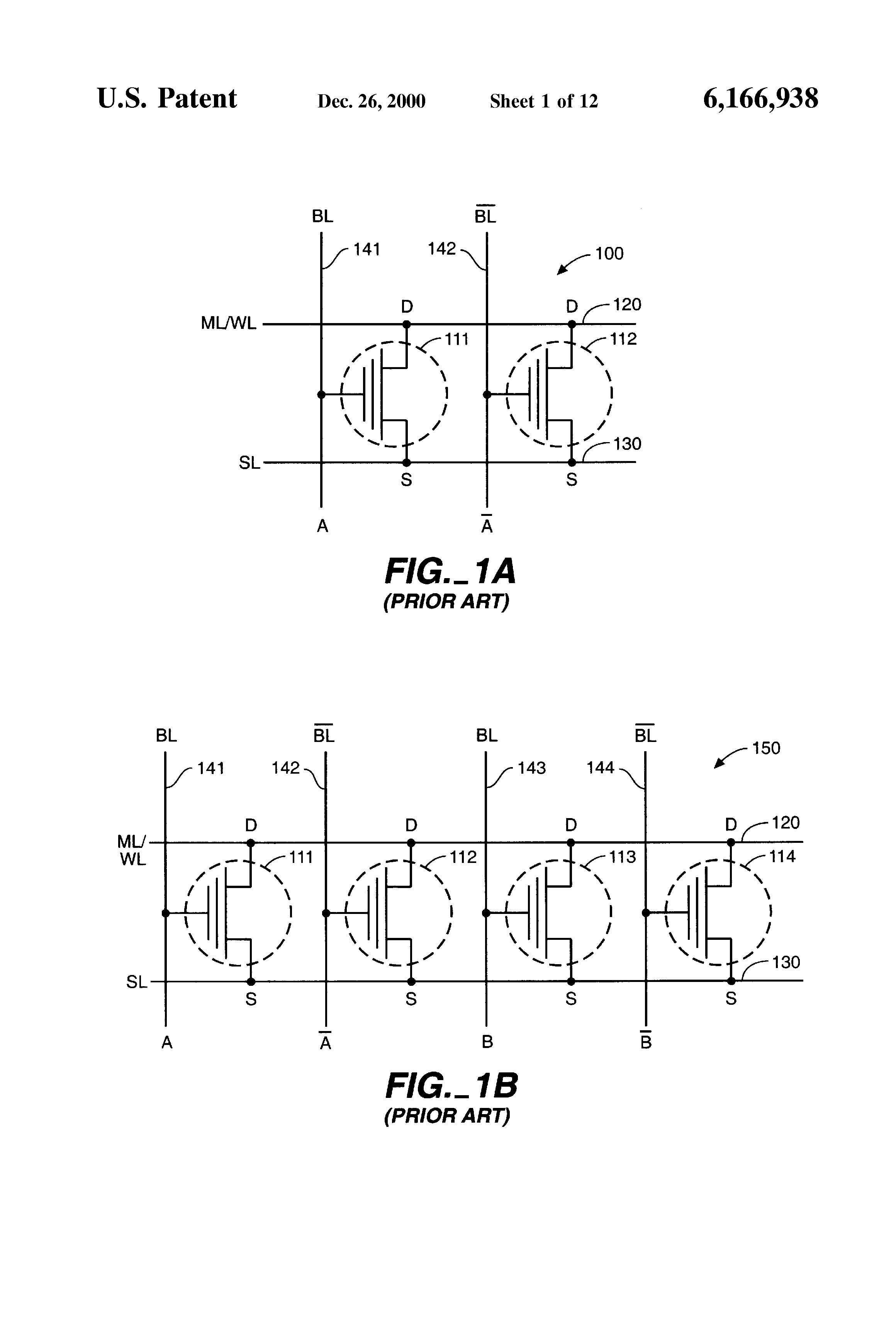
It should be noted that although the above description has focused on arrays based on the 4-T CAM cell 210 of FIG. 2, other 4-T CAM cells are also suitable with the present invention, such as, but not limited to, the two 2-T CAM cell 150 described above with respect to FIG. 1B. FIG. 10 shows an AND input partitioning logic used in conjunction with CAM cell 150. AND input partitioning logic includes four two-input AND gates 1010 coupled to corresponding bit-line drivers 101-104, which are coupled to bit-lines 141-144, respectively. Each of four distinct pairs of input signals A and B and their complements are input to AND gates 1010. Depending on the value of signals A and B, a unique set of signals are applied to bit-line drivers (BLDs) 101-104, as shown in Table 9.
As seen from Table 9, the input to one distinct bit-line driver is high for each of the four AB bit-pair combinations, thereby allowing transistors attached to a particular bit-line driver to be programmed or searched corresponding to one of the four bit-pair combinations, as with the above-described partitioning logic. Thus, according to one convention, transistor 114 (attached to BLD 104) being programmed indicates 00 stored in CAM cell 150, transistor 112 (attached to BLD 102) being programmed indicates 01 stored in CAM cell 150, transistor 113 (attached to BLD 103) being programmed indicates 10 stored in CAM cell 150, and transistor 111 (attached to BLD 101) being programmed indicates 11 stored in CAM cell 150. Searches for bit-pairs 00, 01, 10, and 11 are also accomplished with input partitioning logic, similar to that described above with CAM cell 210, except that the signals applied to bit-lines 141-144 are "opposite" to that applied to bit-lines 241-244. For example, during a search for 00, Vcc is applied to bit-lines 241-243 and ground is applied to bit-line 244 when using CAM cell 210 (see Table 4), while ground is applied to bit-lines 141-143 and Vcc is applied to bit-line 144 using CAM cell 150. Table 10 below summarizes stored and input search bits and some of the parameters when using CAM cell 150 during a search.
As seen from comparing Tables 4 and 10, in order to achieve a "match", programming voltages (which correspond to the threshold voltage) and search voltages applied to the bit-lines are of the same polarity when using CAM cell 210 of FIG. 2, while programming and search voltages are of the opposite polarity when using CAM cell 150 of FIG. 1B. However, similar to using CAM cell 210, bit-line voltages using CAM cell 150 toggle only twice between any two search patterns for a stored bit-pair. Therefore, the benefits of the present invention are also realized with input partitioning logic applied to conventional non-volatile Flash CAM cells, such as CAM cell 150.
In addition to non-volatile CAM arrays, input partitioning logic of the present invention can also be used with volatile CAM arrays comprised of dynamic random accessed memory (DRAM) cells, such as the DRAM CAM cell 1100 shown in FIG. 11. Two transistors 1111 and 1112 are coupled together via capacitors C1 and C2 from a drain of one to a source of the other. The other source and drain terminal of transistors 1111 and 1112 are coupled to respective bit- lines 1141 and 1142. A transistor 1150 is connected as a diode between a match-line 1130 and the common drain of transistors 1115 and 1116, which have sources connected to bit- lines 1141 and 1142. The gates of transistors 1111 and 1112 are connected to a word-line 1120. Capacitors C1 and C2 store the charge, which represent the data (on bit-lines 1141 and 1142) written by transistors 1111 and 1112, respectively. The other terminals of C1 and C2 are connected to a signal CP, which can be either at a "1" or a "0" level.
A "1", "0", or "don't care" state is stored as charge on capacitors C1 and C2. This charge is stored during a write operation by respective transistors 1111 and 1112. During a write operation, word-line 1120 is raised to a "high" level. To store a "1" in DRAM cell 1100, bit-line 1141 is raised to a "high" level and bit-line 1142 is at a "low" level. The high potential on bit-line 1141 charges the gate of transistor 1115 through transistor 1111, i.e., node A is charged high, and the data is thereby stored as a charge on capacitor C1. Similarly, the "low" level (e.g., ground potential) on bit-line 1142 causes the gate of transistor 1116 to discharge to a low level through transistor 1112, i.e., node B is discharged low, thereby discharging capacitor C2. When transistors 1111 and 1112 are subsequently turned off by a low signal on word-line 1120 at the end of a write operation, the charge is trapped or stored on capacitors C1 and C2 at nodes A and B, respectively. This storage convention stores a "0" in DRAM CAM cell 1100 when node A is low and node B is high and stores a "1" in DRAM CAM cell 1100 when node A is high and node B is low. Masking occurs when both nodes A and B are at a low potential, resulting in a "don't care" state.
Because the data in the CAM cell is stored on capacitors, the cell needs to be "refreshed" periodically due to leakage from the capacitors, which can cause errors in reading the data. Refresh cycles, as are well known, maintain proper voltage levels at nodes A and B to ensure the levels correspond to desired values of "1" and "0" when read. During a refresh cycle, bits stored in a word are read and rewritten, i.e., charge is stored on capacitors C1 and C2 by transistors 1111 and 1112, respectively, as determined by the read operation. The frequency of refresh cycles depends on various factors, such as the leakage characteristics at nodes A and B and the capacitance value of capacitors A and B. When a refresh operation is taking place, a search operation cannot be performed. Consequently, an on-chip refresh controller (not shown) typically "arbitrates" between when the DRAM CAM cell is performing refresh, search, and write operations.
A search operation biases match-line 1130 with a low-current, voltage source and applies complementary binary signals to bit- lines 1141 and 1142 to represent the bits of an input value. If bit-line 1141 is high and node A is high, no current flows through transistor 1115 because of the high potential at both the source and the drain of transistor 1115, thereby preventing discharge of the voltage on the match-line 1130. In this situation, bit-line 1142 is low and node B is low, which results in transistor 1116 being off, thereby preventing match-line 1130 from being pulled low by bit-line 1142. This results in a "match". If node A is low and node B is high, with bit-line 1141 low and bit-line 1142 high, no current flows to match-line 1130 because both transistors 1115 and 1116 are off. Thus, match-line 1130 is again prevented from discharging voltage. This also results in a "match". However, if node A is high and bit-line 1141 is grounded, and node B is low and bit-line 1142 is high, voltage on match-line 1130 is discharged via transistors 1115 and 1150. This voltage drop on match-line 1130 indicates a mismatch between the stored data and the input search data. A similar situation occurs when node A is low, bit-line 1141 is high, node B is high, and bit-line 1142 is grounded, where voltage on match-line 1130 is discharged via transistors 1116 and 1150, indicating a "mismatch". In a "don't care" state, indicated by an "X", the voltage at nodes A and B are both low, which leaves transistors 1115 and 1116 turned off, thereby preventing current flow through the transistors to discharge match-line 1130. Consequently, a match is indicated regardless of the input data on the complementary bit- lines 1141 and 1142. Table 11 below indicates the possible combinations of stored and input data bits and some of the parameters of DRAM CAM cell 1100 during a search.
Transistor 1150, acting as a diode, minimizes unwanted parasitic current paths between memory cells of an array. If match-line 1130 were directly coupled to the drains of transistors 1115 and 1116, a transistor (1115 or 1116) which draws current when a mismatch occurs might draw current through a transistor(s) from another bit-line(s) of another CAM cell(s) connected to the same match-line 1130. For example, without transistor 1150, current might flow from a bit-line that is at a high potential coupled to an adjacent DRAM CAM cell (i.e., adjacent transistor), through match-line 1130 and up to a transistor coupled to a mismatched DRAM CAM cell coupled to a bit-line at a low potential. This results in excessive current flow and reduced voltage swing on match-line 1130, which can adversely affect search operations. However, with transistor 1150 acting as a diode connected between match-line 1130 and transistors 1115 and 1116, reverse current is prevented from flowing through adjacent transistors.
Similar to the 2-T non-volatile Flash CAM cell 100 of FIG. 1A, DRAM CAM cell 1100 can be combined with another DRAM CAM cell for storing and searching pairs of data bits. However, as with the two 2-T CAM cell 150 of FIG. 1B, searching pairs of data bits stored in the DRAM CAM cell requires up to four voltage transitions on the four bit-lines between searches. Therefore, the DRAM CAM cell storing pairs of data bits is subject to the similar large A.C. power consumption requirements as with the two 2-T Flash CAM cell 150 of FIG. 1B, described above. By applying an input partitioning logic to the DRAM CAM cell, power consumption can be substantially reduced.
FIG. 12 shows two DRAM CAM cells 1100 forming a DRAM CAM cell 1210 for storing and searching pairs of data bits. CAM cell 1210 includes transistors coupled to four respective bit-lines 1241-1244. Input partitioning logic 1205, according to one embodiment, includes four two-input OR gates coupled to bit-line drivers 1201-1204, which are coupled to respective bit-lines 1241-1244. The OR input partitioning logic is discussed above in conjunction with Table 6. Each of four distinct pairs of input signals A and B and their complements are input to partitioning logic 1205. Depending on the value of signals A and B, a unique set of signals are applied to bit-line drivers (BLDS) 1201-1204 to store a corresponding unique set of four voltages at nodes A, B, C, and D. For example, for storing bit pair 00 (i.e., AB=00), a low signal is applied to bit-line 1241 and high signals are applied to bit-lines 1242-1244, which stores respective low, high, high, and high voltages at nodes A, B, C, and D. Searching is performed similarly, Table 12 shows the possible combinations of stored and input search bits and some of the parameters of DRAM CAM cell 1210 during a search using OR partitioning logic.
As seen from Table 12, only two transitions occur on the bit-lines during searches, thereby reducing power consumption, similar to the discussion above with respect to Flash CAM cells.
Table 13 summarizes bit-line voltages for some of the CAM cells described above for writing and searching bit-pairs 00, 01, 10, and 11, where the columns identify the bit-lines that are high (unless otherwise indicated) for the corresponding write and search operations for each bit-pair.
As seen from Table 13, for write and search operations (both for data encoding and no encoding), the polarity of voltages applied to the bit-lines are the same for CAM cell 150 and DRAM CAM cell 1210, and are the opposite for CAM cell 210. Thus, when utilizing CAM cell 210, tri-state drivers must also be able to invert the polarity of signals applied between search and write operations.
Although the invention has been described with reference to particular embodiments, the description is only an example of the invention's application and should not be taken as a limitation. Various other adaptations and combinations of features of the embodiments disclosed are within the scope of the invention as defined by the following claims.