Skip to content

Patent drawings

Drawing 1 of 4

US 6,363,008

Drawing 1 of 4

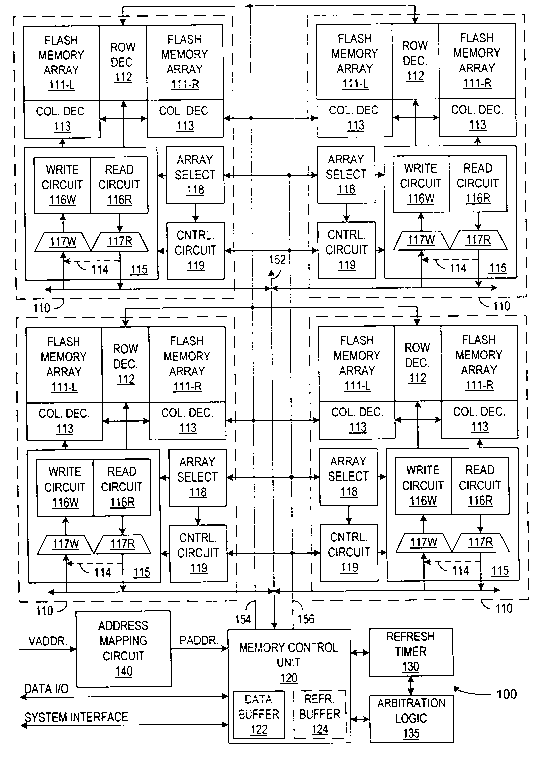
Expanded drawing 1 of 4 from US 6,363,008, Multi-bit-cell non-volatile memory with maximized data capacity
High-resolution patent drawing

US 6,363,008

Multi-bit-cell non-volatile memory with maximized data capacity

Filed
February 17, 2000
Granted
March 26, 2002
Assignee
Samsung
Previous Assignee
MLM
Inventors
Sau-Ching Wong

Abstract

A multiple-bit-per-cell memory includes multiple memory arrays, where the number of bits stored per cell is separately set for each of the memory arrays. Memory arrays that testing proves are accurate when writing, storing, and reading a larger number of bits per cell are set to store more bits per cell, and memory arrays that cannot accurately write, store, or read as many bits per cell are set to store fewer bits per cell. Accordingly, the setting of the numbers of bits per cell for the respective memory arrays can maximize the capacity of a memory when some arrays perform better than expected. When the memory arrays on average perform worse than expected, the setting of the numbers of bits per cell salvage the memory device even if the memory is unable to provide the total expected memory capacity. One implementation of the memory includes a register for the settings of the memory arrays and one or more analog/multi-level write and read circuits. One or more converters convert between the analog and digital signals where the digital signals contain a number of bits selected according to a memory array being accessed. A data buffer between the arrays and a data input/output interface collects data for conversion between the variable data sizes used in the memory and standard size data units input and output from the memory.

View on Google Patents ↗
View Full PatentComplete archived record · 4 figures · 47 description paragraphs · 30 claims

Patent record

Source
Google Patents
Publication
US6363008B1
Application
US09/505,519
Priority
February 17, 2000
Prior art date
February 17, 2000
Publication date
March 26, 2002
Legal status
Expired - Lifetime
Original assignee
Multi Level Memory Technology
Current assignee
Samsung Electronics Co Ltd
Prior art keywords
memory, data, bits, array, cell
Source retrieved
July 20, 2026

Classifications

  • GPHYSICS
  • G11INFORMATION STORAGE
  • G11CSTATIC STORES
  • G11C16/00Erasable programmable read-only memories
  • G11C16/02Erasable programmable read-only memories electrically programmable
  • G11C16/06Auxiliary circuits, e.g. for writing into memory
  • G11C16/10Programming or data input circuits
  • G11C16/20Initialising; Data preset; Chip identification
  • G11C11/00Digital stores characterised by the use of particular electric or magnetic storage elements; Storage elements therefor
  • G11C11/56Digital stores characterised by the use of particular electric or magnetic storage elements; Storage elements therefor using storage elements with more than two stable states represented by steps, e.g. of voltage, current, phase, frequency
  • G11C11/5621Digital stores characterised by the use of particular electric or magnetic storage elements; Storage elements therefor using storage elements with more than two stable states represented by steps, e.g. of voltage, current, phase, frequency using charge storage in a floating gate
  • G11C2211/00Indexing scheme relating to digital stores characterized by the use of particular electric or magnetic storage elements; Storage elements therefor
  • G11C2211/56Indexing scheme relating to G11C11/56 and sub-groups for features not covered by these groups
  • G11C2211/564Miscellaneous aspects
  • G11C2211/5641Multilevel memory having cells with different number of storage levels

Figures

4 plates

Figure 1 of 4 from US 6,363,008, Multi-bit-cell non-volatile memory with maximized data capacity
Figure 01Full resolution ↗
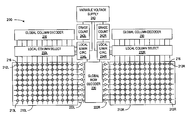
Figure 2 of 4 from US 6,363,008, Multi-bit-cell non-volatile memory with maximized data capacity
Figure 02Full resolution ↗
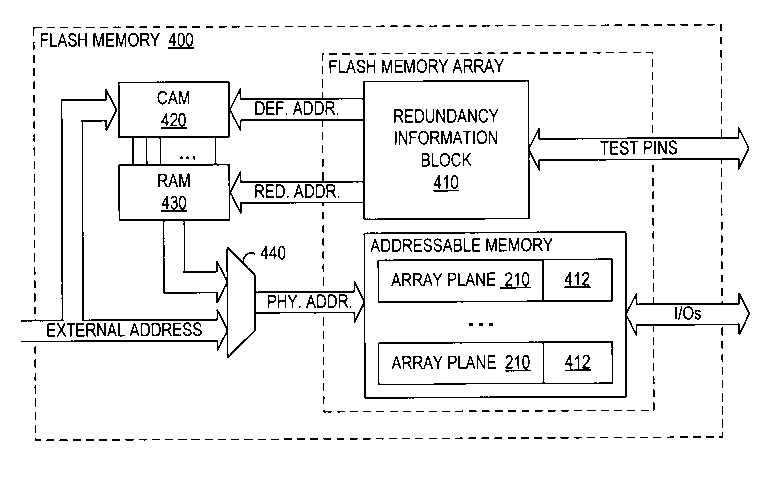
Figure 3 of 4 from US 6,363,008, Multi-bit-cell non-volatile memory with maximized data capacity
Figure 03Full resolution ↗
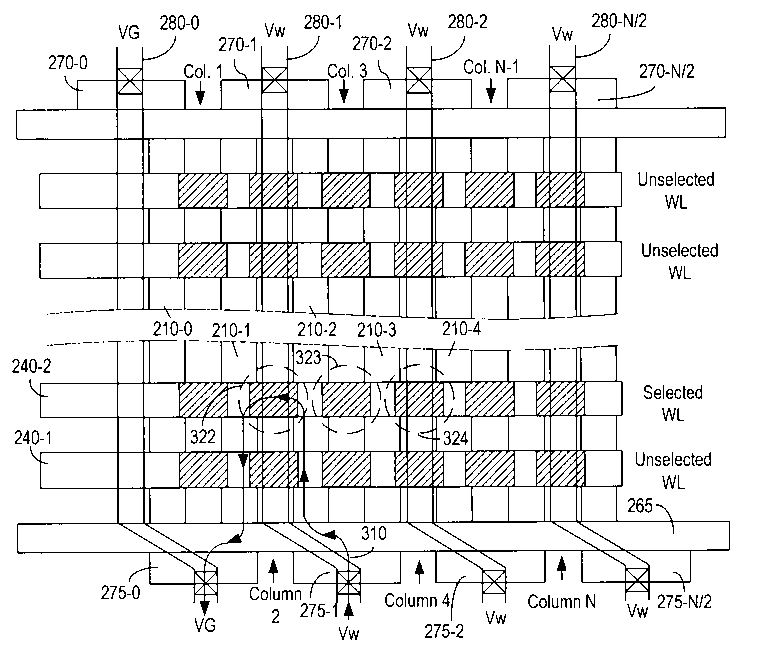
Figure 4 of 4 from US 6,363,008, Multi-bit-cell non-volatile memory with maximized data capacity
Figure 04Full resolution ↗

Description

BACKGROUND

1. Field of the Invention

This invention relates to multi-bit-per-cell non-volatile memory and to methods for classifying and operating such memories for maximum data capacity.

2. Description of Related Art

A traditional semiconductor memory device such as an SRAM, DRAM, ROM, EPROM, Flash, EEPROM, or NVRAM has a data capacity (e.g., 1 Mbit or 1 Gbit) that is pre-determined by the memory device's design. For a multi-bit-per-cell Flash memory, each design/mask-set fixes both the number N of bits stored per cell and the total storage capacity of the Flash memory. For example, a memory designed to store four bits per memory cell and include 64 Meg (1024×1024) cells has a data capacity of 256 Mbits. This data capacity is fixed for the lifetime of the memory. If during manufacturing or operation the memory has fewer than 64 Meg cells that are capable of storing four bits per cell, the memory is defective and must be discarded during manufacture or replaced during operation. This reduces the yield and/or the usable life of multi-bit-per cell memories.

In the design of multi-bit-per-cell Flash memory, there is usually a trade-off between the number of bits N stored per cell and the error rate or data integrity/reliability that the memory provides. Generally, the number N of bits that can be stored per cell depends on the usable range of threshold voltages representing data values and the separation between consecutive threshold voltages that represent different data values. For current memory cell designs, the available threshold voltage range is less than about 5 volts. However, an infinite number of different threshold voltage levels are possible if read and write circuits are perfectly accurate and perfectly calibrated and the memory cells did not experience any threshold voltage drift. In an actual device, several factors limit the minimum separation between distinct threshold voltage levels. In particular, minimum separation must include a margin for charge-gain and charge-loss effects and data retention and endurance effects that change the threshold voltage of memory cells. Additionally, the write and read processes have limited accuracy, which can be affected by parasitic effects across the memory array, such as source line, word line, or bit line resistance, capacitance, and RC effects. Process variations can also lead to unequal performance and reactions for read and write circuits and memory cells. Sensitivities to power supply voltage and temperature provide transient effects that disturb the accuracy with which threshold voltages are read or written. A design for a multi-bit-per-cell memory must account for all of these factors and select a number N of bits that can be stored with a desired reliability.

Assuming a threshold voltage dynamic range of 3.2 V, conventional binary or 1-bit-per-cell Flash memory (N=1) has 2 levels with a threshold voltage window about 1.6 V wide for each level. A two-bit-per-cell memory (N=2) has four levels and an 800 mV wide window for each level. A four-bit-per-cell memory (N=4) has sixteen levels and a 200 mV wide window for each level. As the number of bits per cell increases, the threshold voltage window for each level narrows, and the capability of read and write circuits to distinguish between levels must correspondingly increase if reliability is to be maintained. In addition, the potential for data errors caused by small drifts in the threshold voltages increases as the window for each level narrows. Accordingly, threshold voltage drift must be more tightly controlled as the number N of bits stored per memory cell increases.

Generally, achieving the same reliability or error rate with a two-bit-per-cell memory as with a binary memory is difficult because a fraction of the memory cells in high density memories normally fail to meet all of the stringent requirements for reliably storing two bits of data. Achieving the same reliability with a three- or four-bit-per-cell memory is even more difficult. Further, non-volatile memories such as Flash memories have established quality expectations of minimum data retention time (about 10 years), minimum endurance (>100,000 write/erase cycles), and operability with supply voltage variations (±10%), and temperature variation (0 to 70° C.). The industry established expectations are based on the binary memory architecture and are more difficult to achieve in a multi-bit-per-cell memory.

Several crucial improvements of a proven 1-bit-per-cell memory design are generally required to achieve an N-bit-per-cell memory design with acceptable reliability. The read and write circuits must be modified to significantly improve the threshold voltage write and read accuracy. Assuming that data retention, charge-gain and charge-loss effects are intrinsic and cannot be totally eliminated, extensive tracking or reference circuitry must be added to reduce sensitivities to disturb and aging effects and to supply voltage, temperature, and process variations. Memory array architectures and memory cell and memory cell/array layouts must be tailored to minimize cell-to-cell, array-to-array, and die-to-die variations and disturb and endurance effects.

SUMMARY

In accordance with the invention, a memory device includes multiple memory arrays. Each memory array is operable in multiple modes with each mode corresponding to a different number of bits stored per memory cell in the array. The number of bits stored per cell in each array can be selected based on results of a wafer-sort or a package level test and extrapolation based on a burn-in/life test. The memory device provides lower cost per bit of storage because the memory device can maximize the effective data storage of each array and can salvage memory devices that would otherwise be classified as defective when one or more of the arrays cannot provide a desired storage density. The memory device is particularly useful for mass data storage applications that store serial data because a serial data stream can be broken into data units of variable widths according to the number of bits Nj stored in each memory cell of the receiving array j.

The memory devices can be packaged with a minimum guaranteed memory density with a fixed N across all memory arrays, or with an option to select a highest possible memory density with a different number of bits stored in at least some of the memory arrays. The fixed N option may simplify random memory accesses, but the variable N provides higher data density. For the high-density option, one array may operate as multi-bit-per-cell storage (N>1), while a second array operates a binary storage (N=1) and a third array is disabled (N=0). An on-chip electronic signature can indicate the combined or total (effective) memory density of the device. The package labeling also indicates the total capacity, and the selling price for each device can then be set individually depending on the capacity.

One embodiment of the invention is a manufacturing method that includes: fabricating an integrated circuit memory device that includes a plurality of memory units; testing each memory unit; and setting each memory unit j for storage of Nj bits per cell. Each memory unit has a design capacity to store a maximum of Nmax bits per memory cell, but for each memory unit j, the setting Nj depends on results of the extensive testing. A total storage capacity of the integrated circuit memory device depends on the settings of the memory units. The design of the memory units provides an expected capacity to store Nav bits per memory unit, which typically is less than Nmax. When testing indicates one of the memory units can accurately write, store, and read more than Nav bits per memory cell, the setting causes that memory unit to store more than Nav bits per cell. When testing indicates one of the memory units cannot accurately write, store, or read Nav bits per memory cell, the setting causes that memory unit to store fewer than Nav bits per cell. Accordingly, memory chips of the same design will end up with different memory capacities according to actual capabilities achieved in the manufacturing and testing processes. This allows production of more value memory chips having higher than expected memory capacity and higher yields of operable chips because memory chips having some memory arrays that do not meet expectations can still be salvaged as valuable devices.

Another embodiment of the invention is a memory including multiple memory arrays, a data input/output interface, and a data buffer. The memory arrays have the same design, but among the memory arrays are a first memory array and a second memory array capable of different levels of storage performance. The first memory array is configured to store N1 bits per memory cell, and the second memory array is configured to store N2 bits per memory cell, where N2 is less than N1 and greater than zero. The data buffer is between the input/output interface and the plurality of memory arrays and collects data read from or to be written to the plurality of memory cells. Accordingly, the data buffer converts between the variable data widths used in the memory, and standard data widths for external circuits.

An externally accessible register can store the settings of the numbers of bits store per cell in the arrays. External accessibility allows a user to examine or change the number of bits stored per cell, and thus allows a trade-off between data accuracy and data capacity. Such changes can, for example, maintain a desired level of data accuracy as the memory ages or decrease accuracy to increase memory capacity in error-tolerant applications, such as music or image storage. These techniques are also fully compatible with error correction schemes such as Reed-Solomon coding so that the decreased accuracy associated with the increased memory capacity does not generate any effective (i.e., uncorrectable) errors.

One implementation of the memory includes write and read circuits having a maximum capacity to write and read Nmax-bit digital values. Each digital value corresponds to a threshold voltage of a corresponding memory cell, but some of the bits of the Nmax-bit values may be inaccurate or vary from one memory access to the next. Converters convert data signals according to the accuracy of the memory arrays being accessed.

Yet another embodiment of the invention is a method for using an integrated circuit memory. The method includes: selecting a first memory array in the integrated circuit memory; identifying a number N1 of bits per cell for the first memory array; and accessing a first selected memory cell in the first memory array. The access of the first selected memory cell transfers N1 bits of data. The method further includes: selecting a second memory array in the integrated circuit memory; identifying a number N2 of bits per cell for the second memory array, wherein N2 differs from N1; and accessing a second selected memory cell in the second memory array. The access of the second selected memory cell transfers N2 bits of data. Accordingly, the memory uses internal accesses of different effective data widths per memory cell. Each access can be a write or read operation, and a register can store settings for identification of the numbers of bits per cell accessed in corresponding memory arrays.

BRIEF DESCRIPTION OF THE DRAWINGS

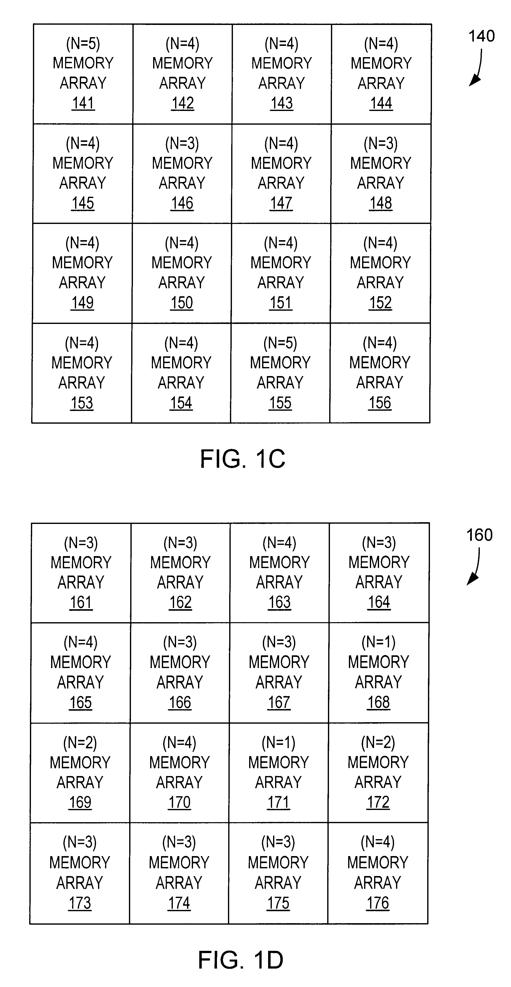
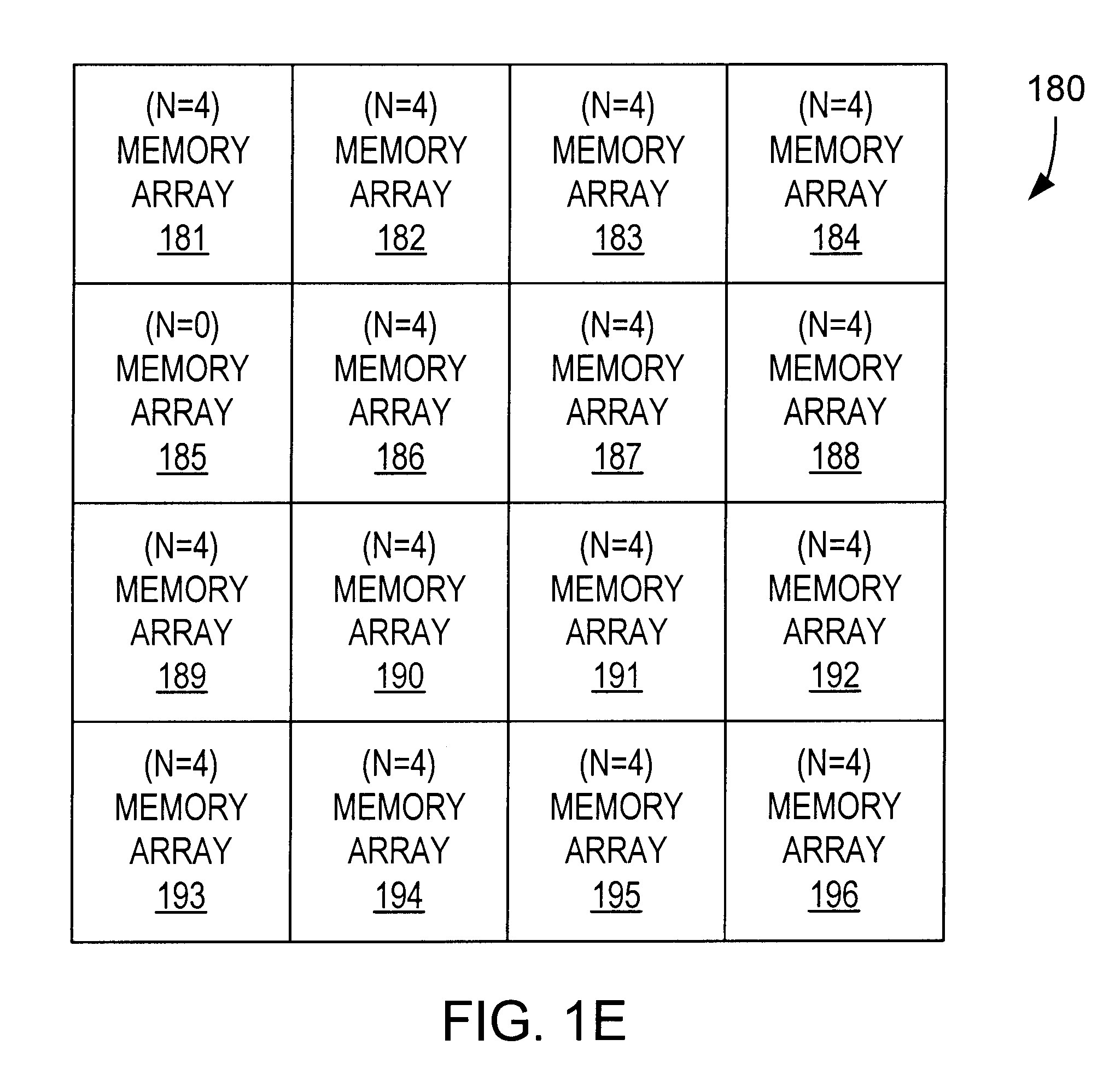
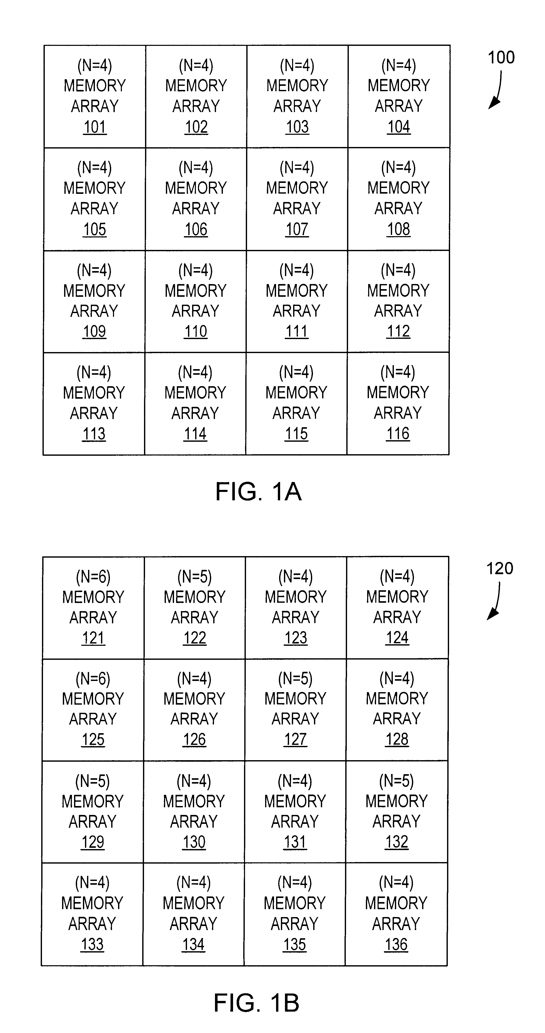
FIGS. 1A, 1B, 1C, 1D, and 1E show memories of identical design that in accordance with the invention are graded at different data capacities.

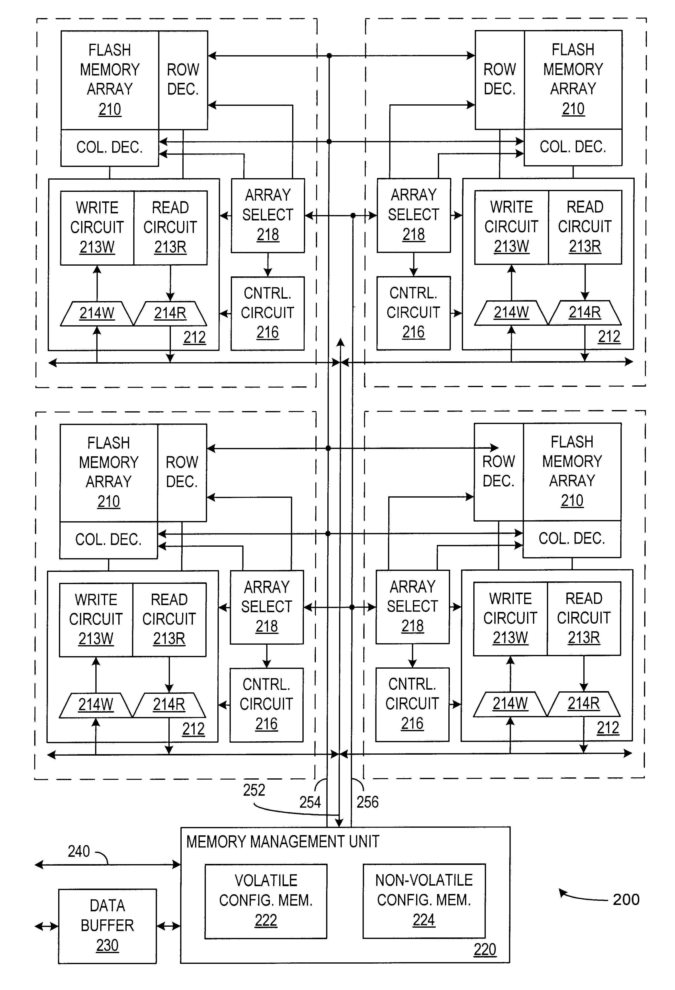
FIG. 2 shows a block diagram or a memory device in accordance with an embodiment of the invention.

FIG. 3 shows a block diagram or a memory device in accordance with another embodiment of the invention.

Use of the same reference symbols in different figures indicates similar or identical items.

DETAILED DESCRIPTION

In accordance with an aspect of the invention, a multi-bit-per-cell memory includes M memory arrays with each memory array j (for j between 1 and M) storing Nj bits per memory cell. Each number Nj depends on the capability of the respective memory array j, which may vary according to variations in an integrated circuit manufacturing process. The values Nj can range between a minimum of zero, indicating the memory array is defective or otherwise not used, to Nmax, which is the maximum number of bits that the read and write circuits can provide when an array performs optimally. The memory architecture is particularly useful for mass data storage that stores blocks of data or a serial data stream at sequential memory addresses. In particular, for writing, a serial data stream of a large data file is broken into data units according to the number of bits that can be written in each memory cell. Different size data units are written in the memory arrays having different numbers of bits per memory cell. Blocks of data are partitioned into data blocks having sizes Nj×Ns where Nj is the number of bits per memory cell and Ns is the number of memory cells per sector in a memory array storing the data block. When reading the serial data or a data block, the data can be reassembled into data units having a conventional size such as 8, 16, 32, or 64 bits wide per data unit.

FIG. 1 is a block diagram of a memory device 100, which includes multiple memory arrays 101 through 116. Each array 101 through 116 includes a fixed number of memory cells, for example, one Meg of memory cells, and is configurable to select the number or bits stored per memory cell. Each of the arrays has associated write, read, and control circuits such as described further below.

The write circuit is designed to write a multi-bit value in a memory cell by setting a threshold voltage of the memory cell to a level corresponding to the value being written. More specifically, the write circuit accepts a multi-bit digital value having up to Nmax bits and programs a memory cell selected for a write operation to one of 2Nmax possible levels. In practice, the write circuit may lack the precision to accurately set threshold voltages at 2Nmax distinct levels. More particularly, when writing the same Nmax-bit value to two different memory cells, the two memory cells may end with different threshold voltages that the read circuit reads as different Nmax-bit values. Additionally, the memory array or specific memory cells in the array may be such that over the life of memory device 100, the threshold voltage drifts, for example, due to charge loss, charge gain, or disturbances during operation of the memory. The drift can take the threshold voltage of a memory cell from one of the 2Nmax levels to another of the levels. To avoid inaccurate writing or changes in stored values, the number Nj of bits stored per memory cell in an array generally must be smaller than Nmax.

The read circuit generates a multi-bit digital value according to the threshold voltage of a memory cell selected for reading. The multi-bit digital value includes Nmax bits, but the one or more of the least significant bits may be unreliable (and therefore unused). More specifically, one or more of the least significant bits may differ during different readings of the same cell through out the life of the memory device 100. Again, to avoid inaccuracies in read values, the number Nj of bits stored (and read) per memory cell in an array generally is smaller than Nmax.

Input and output ports of each array are configurable to select a number of input bits Nj used for a write operation or output after a read operation. Testing of an array indicates the optimal number Nj of bits per cell for the array. Generally, the number Nj is the maximum number of bits that can be accurately written and read from individual memory cells in the array. Programming of the input and output ports can be, for example, by way of laser fuses, poly fuses, or anti-fuse or using non-volatile memory elements to store the number Nj or equivalent repair information. Such fuses and similar structures are commonly employed for repair operations using redundant memory cells in conventional memory. A write circuit still uses an Nmax-bit input value, but the value being written in a memory cell only provides Nj valid bits, typically the Nj most significant bits of the Nmax-bit input value. The least significant bits can be ignored or set to a fixed value (e.g., all 0 or all 1) or to a value that maximizes the distance between the 2Nj levels required for when representing Nj-bit values. The read circuit determines an Nmax-bit read value from the threshold voltage of a selected memory cell and can ignore or truncate the least significant bits of the Nmax-bit value or perform rounding on the Nmax-bit values to generate an N-bit output value.

In an exemplary embodiment of the invention, the maximum number Nmax of input and output bits of the write and read circuits is eight, but the typical memory array in an actual integrated circuit only permits accurate writing and reading of four bits per memory cell. In the memory 100, each of memory arrays 101 to 116 performs as expected and is capable over accurately writing and reading four bits of data per memory cell. Accordingly, the total memory capacity of memory 100 is 64 Mbits (16 arrays×4 bits/cell×1 Meg cells/array).

FIG. 1B shows a memory 120 having the same design as memory 100. Memory 120 differs from memory 100 in that some memory arrays 121, 122, 125, 127, 129, and 132 perform better than expected. Other memory arrays 123, 124, 126, 127, 128, 130, 131, 133, 134, 135, and 136 in memory 120 perform as expected. In particular, memory arrays 121 and 125 are capable of writing and reading 6-bit values with the desired reliability. Memory arrays 122, 127, 129, and 132 can write and read 5-bit values with the desired reliability. Memory arrays 123, 124, 126, 127, 128, 130, 131, 133, 134, 135, and 136 can write and read 4-bit values with the desired reliability. During manufacture, a test determines the capabilities of the memory arrays 121 to 136 and programming of the I/O circuitry of memory 120 selects the numbers of bits for the arrays as given above. As a result, the total memory capacity of the memory array 120 is 72 Mbits {(2 arrays×6 bits/cell+4 arrays×5 bits/cell+10 arrays×4 bits/cell)×1 Meg cells/array}. Accordingly, a multi-bit-per-cell memory design expected to work with 4 bits per cell for a total memory capacity of 64 Mbits can actually provide memory devices with higher capacity (e.g., 72 Mbits), which presumably would command a higher market price. On the other hand, the higher capacity devices can be sold at the same price as the other available 64 Mbit devices, and provide the buyers with the option of more memory capacity.

Memory arrays may also test and perform worse than expected. FIG. 1C shows a memory 140 of the same design as memories 100 and 120 of FIGS. 1A and 1B. In memory 140, arrays 141 and 155 perform better than average and can accurately write, store, and read 5 bits per memory cell. Memory arrays 142-145, 147, 149-154, and 156 perform as expected and can accurately, write, store, and read 4 bits per memory cell. However, memory arrays 146 and 148 perform worse than expected and can accurately, write, store, and read only 3 bits per memory cell. This memory would be defective and discarded in a memory architecture that demands every array to store the four bits per memory cell. However, better performing arrays of the memory 140 compensate for worse performing arrays of memory 140, and memory 140 has a total storage capacity of 64 Mbits {(2 arrays×5 bits/cell+12 arrays×4 bits/cell+2 arrays×3 bits/cell)×1 Meg cells/array}. Accordingly, the variable setting of the number of bits per memory cell allows a higher yield of operable devices having the desired density and reliability.

Even when the arrays on average perform worse than expected, the variable setting of the number of bits per cell can salvage a memory device. FIG. 1D shows a memory device 160 having the same design as memory 100 of FIG. 1, but testing indicates that arrays of memory device 160 on average perform worse than expected. In memory 160, memory arrays 163, 165, 170, and 176 perform as expected and can accurately, write, store, and read four bits per memory cell. The remaining memory arrays perform worse than expected. Memory arrays 161, 162, 164, 166, 167, 173, 174, and 175 can accurately, write, store, and read three bits per memory cell. Memory arrays 169 and 172 can accurately, write, store, and read two bits per memory cell. Memory arrays 168 and 171 can only store one bit per memory cell and effectively operate as binary memory arrays. Accordingly, the total memory capacity of memory 160 is 46 Mbits {(4 arrays×4 bits/cell+8 arrays×3 bits/cell+2 arrays×2 bits/cell+2 arrays×1 bit/cell)×1 Meg cells/array}. Accordingly, instead of discarding memory 160 as being unable to achieve the desired capacity of 64 Mbits, the memory 160 is an economically valuable memory device.

Another feature of the inventions is that a memory device can be economically valuable even if one or more arrays are defective and unable to store any data. FIG. 1E shows a memory device 180 in which one memory array 185 is defective but the other arrays 181 to 184 and 186 to 196 perform as expected and are capable of reliably writing, storing, and reading four bits per cell. The defect in memory array 185 is an unrepairable defect that makes the array unable to store any data in at least some of the addresses of the array. Memory 180 is programmed or configured to store four bits per cell in arrays 181 to 184 and 186 to 196 and no data (zero bits per cell) in array 185. Accordingly, the total capacity of memory 180 is 60 Mbits, and memory 180 is an economically valuable device instead of a device that must be discarded.

FIG. 2 is a block diagram of a multi-bit-per-cell Flash memory 200 in accordance with an embodiment of the invention. Memory 200 includes multiple memory arrays 210. Each array 210 includes rows and columns of memory cells. Each memory cell can be a conventional Flash memory cell (e.g., a floating gate transistor), an EEPROM cell, or an EPROM cell. Row lines (not shown) connect a row decoder to the control gates of memory cells in the rows of memory array 210. Column lines (not shown) connect sense amplifiers and a column decoder to drains of memory cells in the columns of memory array 210. Each array 210 is further divided into erasable sectors, and a source line connects to the sources of memory cells in an associated sector. The implementation of each array 210 and the associated row and column decoders can be conventional for multi-bit-per-cell memory. Memory arrays 210 can each consist of multiple segmented memory banks (not shown), each bank containing multiple sectors. The maximum number of memory cells on a bit-line segment depends on the maximum tolerable program disturb characteristics of the memory cells.

Also associated with each array 210 are multi-bit-per-cell write/read circuit 212, a control circuit 216, and an array selection circuit 218. A data bus 252, an address bus 254, and an array select bus 256 respectively provide data signals, address signals, and array select signals from a memory management unit 220 to the circuitry associated with arrays 210. An external control interface 240 provides control signals for operation of memory 200, and memory data buffer 230 temporarily stores data input to memory 200 or until output from memory 200.

For one embodiment of a write operation; data buffer 230 collects externally input data until data buffer 230 contains enough data to fill an entire sector of a selected memory array. The amount of data stored in a sector of a memory array j depends on the number of memory cells in the sector and the number Nj of bits stored per memory cell. Buffer 230 would normally include at least twice the capacity of a sector in a memory array that can store the maximum number Nmax of bits per memory cell. With this configuration, one portion of buffer 230 can provide the data being written to a sector, while another portion of buffer 230 continues to collect data for writing in the next selected sector. Alternatively, write operations are not required to be on a per sector basis and can begin when buffer 230 contains Nj bits of data to be written.

Memory management unit 220 generates array select signals to select one of the arrays 210 for the write operation. Address signals from the memory management unit 220 then select an erased sector in the array and a selected memory cell in the selected sector. Memory management unit 220 then retrieves an Nj-bit value from data buffer 230, where Nj is the number of bits stored per cell in the selected array. An optional volatile configuration memory 222, which contains volatile memory such as SRAM, can store the number Nj for memory management unit 220. Volatile configuration memory 222 permits configuration at power up of memory 200 and permits a user to override previous selections of the bit limits Nj. For example, at power up, values Nj can be read from non-volatile configuration memory 224 and stored in volatile configuration memory 222. Configuration memory 224 can be a ROM or an electrically programmable non-volatile memory such as Flash memory. A ROM can be programmed, for example, by cutting fuses during manufacture and testing of memory 200. Configuration memory 224 can be a separate array or may consist of memory cells scattered in the arrays 210 if configuration memory 224 uses Flash memory cells. Volatile configuration register 222 can be omitted if values Nj are read directly from non-volatile configuration memory 224 when required. Alternatively, non-volatile configuration memory 224 can be omitted, giving the user complete responsibility for setting volatile configuration memory 222.

Memory management unit 220 constructs an Nmax-bit signal for a write operation, using a corresponding Nj-bit value to be written. More particularly, the Nj-bit value provides the most significant bits of the Nmax-bit signal, and the least significant bits of the Nmax-bit signal can be selected according to a convention implemented in memory management unit 220. For example, the least significant bits can be all zero, all one, or have a value that depends on the Nj-bit value and provides a maximum separation between the Nj-bit values.

The control circuit 216 for the selected memory array 210 enables operation of the write circuitry associated with the selected array. Control circuits 216 for unselected arrays disable the write circuitry in the unselected arrays. In the embodiment, of FIG. 2, the write circuit include a converter 214W that converts the Nmax-bit signal to an analog voltage, and an analog/multi-level write circuit 213W that programs the threshold voltage of a selected memory cell to a target threshold voltage corresponding to the analog voltage. The analog/multi-level write and read circuits 212 connected to the selected array generate the programming voltages necessary to program the selected memory cell to the target threshold voltage. Analog/multi-level read and write circuits are known in the art and described, for example, in U.S. Pat. No. 5,694,356, which is hereby incorporated by reference in its entirety. The particular type of analog/multi-level write circuit used is not critical to the invention, but generally, high accuracy is desired to allow up to 2Nmax different threshold voltage levels.

When the write circuit has programmed the selected memory cell to the target threshold voltage, memory management unit 220 changes the address signal to select the next memory cell in the selected sector and retrieves the next Nj bits from data buffer 230. The write operation programs the newly selected memory cell to the threshold voltage corresponding to the next Nj-bit value. The write operation repeats until an Nj-bit value is written in the last memory cell of the selected sector or writing is otherwise complete. Memory management unit 220 then selects another sector for a write operation. If the new sector is in another array 210, memory management unit 220 changes the array select signal, reads configuration memory 222, and changes the bit limitation Nj if the number of bits stored per cell in the newly selected array differs from the number of bits per cell in the previously selected array. The writing of the sector typically begins when data buffer 230 contains enough data to fill the next data sector but alternatively can start whenever data buffer 230 contains the next Nj bits of data to be written.

For a read operation, memory management unit 220 again generates the array select signal and address signal to select an array, a sector of the selected array, and a memory cell in the selected sector. The control circuit 216 for the selected array 210 directs the associated write and read circuit 212 to read the threshold voltage of the selected memory cell. In the embodiment of FIG. 2, the read circuits include an analog/multi-level read circuit 213R and a converter 214R. Analog/multi-level read circuit 213R provides an analog signal to converter 214R representing the threshold voltage of the selected memory cell, and converter 214R outputs an Nmax-bit digital signal to the Nmax-bit wide data bus 252. Memory management unit 220 receives the Nmax-bit digital signal and extracts Nj bits of data, for example, by ignoring or truncating the least significant bits, by rounding where the least significant bits represent a fraction, or by some other more complex conversion. Data buffer 230 collects the Nj data bits from the selected memory cell. The read operation repeats for each memory cell in the selected sector so that data buffer collects the block of data originally written into the selected sector. The data can then be read out externally via the I/O interface at high speed.

The described embodiment of memory 200 can be varied in many ways. Parallel or pipelined operations can take place among memory arrays 210 or within the same memory array 210. For example, instead of writing one Nj-bit data value at a time, multiple data values having the same or different sizes can be written in parallel using one array 210 or two more arrays 210 in parallel. Alternatively, memory management unit 220 operates arrays 210 in a pipeline fashion by starting a write or read operation in an array 210 before a previously started write or read operation in that or another memory array 210 is complete. Each parallel or pipelined write operation receives an Nmax-bit value where the number Nj of bits representing actual data depends on the capabilities of the target array 210 or more specifically on the values in configuration memory 222. Each read operation similarly provides an Nmax-bit value, where Nj bits are valid and used according to the location of the memory cell read. Parallel or pipelined write and read operations provide a higher bandwidth when recording or playing back a data stream.

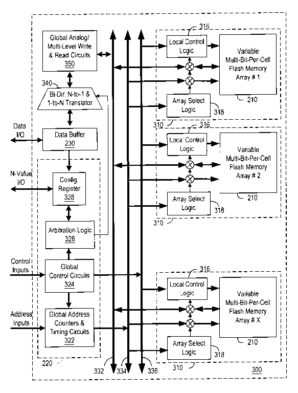
FIG. 3 illustrates an embodiment of a memory 300 that reduces overhead by sharing a converter 340 and global analog/multi-level write and read circuits 350 among multiple memory units 310, each including a memory array 210. Additionally, memory units 310 further reduce overhead by sharing global control circuits 324. Global control circuits 324 generate internal control signals that govern chip operations including erase operations, write operations, read operations, charge pump operations, stand-by mode operations, and various test operations. A typical memory can have more than fifty internal control signals. Local control logic 316 for each array 210 receives global control signals and generates appropriate local control signals that depend on whether the associated array 210 is selected.

To write a data value in a selected memory cell, converter 340 fetches Nj bits from data buffer 230 where Nj is the number of bits that are stored per cell in the selected memory array 210. A configuration register 328 stores the set of values Nj. Converter 350 converts an Nj-bit value from data buffer 230 into an analog voltage representing the value to be written in the selected memory cell. Typically, the conversion depends on the number of bits stored per memory cell in the target array so that the memory array employs the full available range of threshold voltages. Converter 350 provides the analog voltage to the global analog/multi-level write and read circuits 350.

Global analog/multi-level read and write circuits 350 generate the voltages to be applied to the selected memory cell during a write operation. More particularly, global analog/multi-level read and write circuits 350 generate row and column line voltages required for programming, which changes the threshold voltage of the selected memory cell, and row and column line voltages used to verify that the selected memory cell has reached a threshold voltage representing the data value. During a write operation, a global bus 332 carries the row and column line voltages for use by any of memory units 310.

Global address bus 334 carries address signals from global address circuits 322 in memory management unit 220 to all of memory units 310. Part of the address signal is an array select signal. The array select decoder 318 in the selected memory unit 310 recognizes the array select signal and enables use of row and column addresses from global address bus 334 and program and verify voltages from global bus 332. Row and column decoders in the selected array 210 select a memory cell according to the row and column address and apply the row and column line voltages from global bus 332 to the selected memory cell.

Similarly, during a read of a selected memory cell, global address circuits 322 generate an address signal to identify the selected memory array and the selected memory cell. The array select decoder 318 enables the row and column address to reach the row and column decoders of the selected array and connects global write and read circuits 350 to the selected array 210. Global write and read circuits 350 generate an analog signal indicating threshold voltage of the selected memory cell, and apply the signal to converter 340. Converter 340 then converts the analog signal to an Nj-bit data value where Nj is the number of bits per cell stored in the selected array as indicated in configuration register 328. As for a write operation, arbitration logic 326 reads the value Nj from configuration register 328 and controls converter 340 accordingly. Data buffer 230 collects the data values from converter 340 for output in data units of a standard size.

FIG. 3 also illustrates an embodiment of memory management unit 220 that includes global address circuits 322, global control circuits 324, arbitration logic 326, and configuration register 328. Configuration register 328 stores a set of values Nj where index j runs over a range corresponding to arrays 210 in memory 300. For normal operation, the values Nj are from non-volatile memory and loaded into configuration register 328 during start up of memory 300. The non-volatile memory can be a ROM (not shown) or part of arrays 210 in memory 300. The values Nj can be stored in ROM, for example, by setting a fuse option in response to testing memory 300. Programming erasable programmable ROM such as Flash memory with the values Nj allows possible changes in the values that will allow memory 300 to continue to operate even if one or more array 210 becomes unable to store the number of bits that initial testing indicated.

External access to configuration register 328 allows a system's CPU or controller to examine and/or select the number of bits stored per memory cell in each of the arrays. The values Nj from ROM provide a rating of the capability to store information with a particular reliability. If desired, a system can operate memory at a higher data density but a lower than normal reliability, depending on a users selection. Alternatively, based on the value Nj from ROM, the system (or the user) can selectively allocate the memory array with the most appropriate (most effective) value Nk according to the nature of the data. For example, code or program storage, which requires absolute data integrity, could be stored in a memory array 210 rated for storing a large number Nj of bits but using only Nk bits per memory cell where Nk is less than Nj to maximize data integrity. Other types of data can choose a different approach. Further, external access to configuration register 328 allows testing of the arrays by setting the value Nj for an array, writing data to that array, and reading data from that array to determine whether there are any errors.

Global address circuits 322 receive an external address indicating the memory locations or sectors to be accessed (written or read). Address circuit 322 converts the external address to an internal address identifying a first sector or first memory cell storing data corresponding to the external address. A variety of systems for the conversion between external and internal addresses are possible. For example, memory manage management unit 220 can implement a file organization or a sector access organization similar to that employed in disk drives. The external address typically corresponds to a block of data or a data unit that is stored in several memory cells. Counters in global address circuit 322 increment (or otherwise change) the internal address as required for accessing each memory cell associated with the block. The number of memory cells accessed depends on the amount of data transferred and the number Nj of bits stored per memory cell.

Although the invention has been described with reference to particular embodiments, the description is only an example of the invention's application and should not be taken as a limitation. Various adaptations and combinations of features of the embodiments disclosed are within the scope of the invention as defined by the following claims.
Claims (30)

  1. A memory comprising: a plurality of memory arrays including a first memory array and a second memory array, the first memory array being configured to store N1 bits per memory cell, the second memory array being configured to store N2 bits per memory cell, where N2 is less than N1 and greater than zero; a data input/output interface; and a data buffer coupled between the input/output interface and the plurality of memory arrays, the data buffer collecting data read from or to be written to the plurality of memory cells.
  2. The memory of claim 1, wherein: for an operation reading from the first memory array, the data buffer collects N1 bits of data from each memory cell read for subsequent output through the input/output interface; and for an operation reading from the second memory array, the data buffer collects N2 bits of data from each memory cell read for subsequent output through the input/output interface.
  3. The memory of claim 1, wherein: for an operation writing to the first memory array, the data buffer provides N1 bits of data for each memory cell to which data is being written; and for an operation writing to the second memory array, the data buffer provides N2 bits of data for each memory cell to which data is being written.
  4. The memory of claim 1, further comprising a register storing a plurality of values including N1 and N2, wherein each value stored in the register corresponds to one of the plurality of arrays and indicates a number bits stored per memory cell in the corresponding array.
  5. The memory of claim 4, wherein the register is user-accessible for examination of the plurality of values.
  6. The memory of claim 4, wherein the register is user-accessible for changing the plurality of values.
  7. The memory of claim 4, wherein the register comprises non-volatile memory storing the plurality of values.
  8. The memory of claim 1, further comprising a read circuit coupled to the second memory array, the read circuit generating an Nmax-bit value according to a threshold voltage of a selected memory cell in the second memory array, wherein Nmax is greater than N2.
  9. A memory comprising: a plurality of memory units, each memory unit comprising: a memory array; a write circuit that receives an Nmax-bit value and programs a threshold voltage of a memory cell in the array, to a target level selected according to the Nmax-bit value; and a read circuit that generates an Nmax-bit value according to a threshold voltage of a memory cell being read; a global data bus coupled to provide Nmax-bit values to the write circuits and receive Nmax-bit values from the read circuits; and input/output circuitry coupled to the global data bus, the input/output circuitry selecting a number of bits on the global data bus that are actual data, the number of bits depending on which of the plurality of memory units is involved in a data transfer on the global data bus.
  10. The memory of claim 9, further comprising a configuration register coupled to the input/output circuitry, the configuration register containing configuration values indicating for each memory unit, a number of data bits stored per memory cell in that memory unit.
  11. The memory of claim 10 wherein the configuration register is user-accessible for examination of the configuration values.
  12. The memory of claim 10 wherein the configuration register is user-accessible for changing of the configuration values.
  13. The memory of claim 10, wherein the configuration register comprises non-volatile memory storing the configuration values.
  14. A memory comprising: a plurality of memory units; a global write/read circuit coupled to the plurality of memory units to control writing to and reading from the plurality of memory units; input/output circuitry coupled to the global write/read circuit, the input/output circuitry selecting a number of bits of actual data transferred by a write or read operation, the number of bits depending on which of the plurality of memory units is the target of the write or read operation; and a converter coupled to the global write/read circuit, wherein the converter converts a first digital signal to an analog signal representing a value for a write operation that the global write/read circuit controls, the digital signal containing a number of data bits selected by the input/output circuitry; and the converter converts an analog signal from the global write/read circuit to a second digital signal, the second digital signal containing a number of data bits selected by the input/output circuitry.
  15. A memory comprising: a plurality of memory units; a global write/read circuit coupled to the plurality of memory units to control writing to and reading from the plurality of memory units; input/output circuitry coupled to the global write/read circuit, the input/output circuitry selecting a number of bits of actual data transferred by a write or read operation, the number of bits depending on which of the plurality of memory units is the target of the write or read operation; and a configuration register coupled to the input/output circuitry, the configuration register containing configuration values indicating for each memory unit, a number of data bits stored per memory cell in that memory unit.
  16. The memory of claim 15 wherein the configuration register is user-accessible for examination of the configuration values.
  17. The memory of claim 15 wherein the configuration register is user-accessible for changing of the configuration values.
  18. The memory of claim 15, wherein the configuration register comprises non-volatile memory storing the configuration values.
  19. A method for using an integrated circuit memory, comprising: selecting a first memory array in the integrated circuit memory; identifying a number N1 of bits per cell for the first memory array; accessing a first selected memory cell in the first memory array, wherein the access of the first selected memory cell transfers N1 bits of data; selecting a second memory array in the integrated circuit memory; identifying a number N2 of bits per cell for the second memory array, wherein N2 differs from N1; and accessing a second selected memory cell in the second memory array, wherein the access of the second selected memory cell transfers N2 bits of data.
  20. The method of claim 19, wherein: identifying the number N1 comprises reading the number N1 from a first register entry that corresponds to the first memory array; and identifying the number N2 comprises reading the number N2 from a second register entry that corresponds to the second memory array.
  21. The method of claim 20, wherein the first and second register entries are in a volatile memory.
  22. The method of claim 21, further comprising a start-up procedure for the memory, the start-up procedure comprising: reading the values N1 and N2 from non-volatile memory; and storing the numbers N1 and N2 in the volatile memory.
  23. The method of claim 21, a user writing the numbers N1 and N2 to the volatile memory to select a storage density for the first and second memory units.
  24. The method of claim 19, wherein: accessing the first selected memory cell comprises reading the first selected memory cell to determine an N1-bit value that corresponds to a threshold voltage of the first selected memory cell; and accessing the second selected memory cell comprises reading the second selected memory cell to determine an N2-bit value that corresponds to a threshold voltage of the second selected memory cell.
  25. The method of claim 19, wherein: accessing the first selected memory cell comprises writing to the first selected memory cell to set a threshold voltage of the first selected memory cell to a level corresponding to an N1-bit value; and accessing the second selected memory cell comprises writing to the second selected memory cell to set a threshold voltage of the second selected memory cell to a level corresponding to an N2-bit value.
  26. A method for using a non-volatile integrated circuit memory, comprising: configuring the non-volatile integrated circuit memory by writing a value N1 in a first register entry corresponding to a first memory unit in the non-volatile integrated circuit memory; and accessing a first selected memory cell in the first memory unit, wherein the value N1 indicates a number of data bits that the access transfers to or from the first selected memory cell.
  27. The method of claim 26, further comprising: writing a value N2 in a second register entry corresponding to a second memory unit in the non-volatile integrated circuit memory; and accessing a second selected memory cell in the second memory unit, wherein the access of the second selected memory cell transfers N2 bits of data.
  28. The method of claim 27, wherein N2 differs from N1.
  29. The method of claim 26, wherein the configuring is performed during a start-up procedure for the non-volatile integrated circuit memory.
  30. The method of claim 26, wherein the configuring is performed by inputting a signal that represents the value N1, into the non-volatile integrated circuit memory.

Publications

Related applications (5)

  1. US09/505,519

    Priority application

  2. US09/775,415

    Priority application

  3. US09/505,519

    Claims priority

  4. US09/505,519

    Patent family

  5. US09/775,415

    Patent family

Record timeline

  1. Application filed by Multi Level Memory Technology

  2. Priority to US09/505,519

  3. Assigned to MULTI LEVEL MEMORY TECHNOLOGY

  4. Priority to US09/775,415

  5. Application granted

  6. Publication of US6363008B1

  7. Assigned to MULTI LEVEL MEMORY TECHNOLOGY (NEVADA)

  8. Assigned to INTERNATIONAL DEVELOPMENT AND LICENSING

  9. Assigned to SAMSUNG ELECTRONICS CO., LTD.

  10. Anticipated expiration

  11. Expired - LifetimeCurrent

Legal events

  1. AS

    Assignment

    Owner name: MULTI LEVEL MEMORY TECHNOLOGY, CALIFORNIA

    Free format text: ASSIGNMENT OF ASSIGNORS INTEREST;ASSIGNOR:WONG,SAU-CHING;REEL/FRAME:010624/0984

    Effective date: 20000217

  2. STCF

    Information on status: patent grant

    Free format text: PATENTED CASE

  3. FEPP

    Fee payment procedure

    Free format text: PAT HOLDER NO LONGER CLAIMS SMALL ENTITY STATUS, ENTITY STATUS SET TO UNDISCOUNTED (ORIGINAL EVENT CODE: STOL); ENTITY STATUS OF PATENT OWNER: LARGE ENTITY

  4. REFU

    Refund

    Free format text: REFUND - SURCHARGE, PETITION TO ACCEPT PYMT AFTER EXP, UNINTENTIONAL (ORIGINAL EVENT CODE: R2551); ENTITY STATUS OF PATENT OWNER: LARGE ENTITY

  5. AS

    Assignment

    Owner name: MULTI LEVEL MEMORY TECHNOLOGY (NEVADA), NEVADA

    Free format text: ASSIGNMENT OF ASSIGNORS INTEREST;ASSIGNOR:MULTI LEVEL MEMORY TECHNOLOGY (CALIFORNIA);REEL/FRAME:016800/0640

    Effective date: 20050720

  6. AS

    Assignment

    Owner name: INTERNATIONAL DEVELOPMENT AND LICENSING, CALIFORNI

    Free format text: ASSIGNMENT OF ASSIGNORS INTEREST;ASSIGNOR:MULTI LEVEL MEMORY TECHNOLOGY;REEL/FRAME:017176/0517

    Effective date: 20050802

  7. FPAY

    Fee payment

    Year of fee payment: 4

  8. AS

    Assignment

    Owner name: SAMSUNG ELECTRONICS CO., LTD., KOREA, REPUBLIC OF

    Free format text: ASSIGNMENT OF ASSIGNORS INTEREST;ASSIGNOR:INTERNATIONAL DEVELOPMENT AND LICENSING;REEL/FRAME:017230/0319

    Effective date: 20050804

  9. FEPP

    Fee payment procedure

    Free format text: PAYOR NUMBER ASSIGNED (ORIGINAL EVENT CODE: ASPN); ENTITY STATUS OF PATENT OWNER: LARGE ENTITY

  10. FPAY

    Fee payment

    Year of fee payment: 8

  11. FPAY

    Fee payment

    Year of fee payment: 12

Patent citations (71)

  1. US5095344A

    Highly compact eprom and flash eeprom devices

    Eliyahou Harari · March 10, 1992

  2. US5043940A

    Flash EEPROM memory systems having multistate storage cells

    Eliyahou Harari · August 27, 1991

  3. US5293560A

    Multi-state flash EEPROM system using incremental programing and erasing methods

    Eliyahou Harari · March 8, 1994

  4. US5262984A

    Non-volatile memory device capable of storing multi-state data

    Mitsubishi Denki Kabushiki Kaisha · November 16, 1993

  5. US5511022A

    Depletion mode NAND string electrically erasable programmable semiconductor memory device and method for erasing and programming thereof

    Samsung Electronics Co., Ltd. · April 23, 1996

  6. US5097445A

    Semiconductor integrated circuit with selective read and write inhibiting

    Mitsubishi Denki Kabushiki Kaisha · March 17, 1992 · Examiner cited

  7. US5172338A

    Multi-state EEprom read and write circuits and techniques

    Sundisk Corporation · December 15, 1992

  8. US5163021A

    Multi-state EEprom read and write circuits and techniques

    Sundisk Corporation · November 10, 1992

  9. US5172338B1

    Multi-state eeprom read and write circuits and techniques

    Sandisk Corp · July 8, 1997

  10. US5877986A

    Multi-state Flash EEprom system on a card that includes defective cell substitution

    Sandisk Corporation · March 2, 1999

  11. US6149316A

    Flash EEprom system

    Sandisk Corporation · November 21, 2000

  12. US5239506A

    Latch and data out driver for memory arrays

    International Business Machines Corporation · August 24, 1993

  13. US5504760A

    Mixed data encoding EEPROM system

    Sandisk Corporation · April 2, 1996

  14. US6011741A

    Computer memory cards using flash EEPROM integrated circuit chips and memory-controller systems

    Sandisk Corporation · January 4, 2000

  15. US6016530A

    Mass computer storage system having both solid state and rotating disk types of memory

    Sandisk Corporation · January 18, 2000

  16. US6222762B1

    Multi-state memory

    Sandisk Corporation · April 24, 2001

  17. US5371702A

    Block erasable nonvolatile memory device

    Kabushiki Kaisha Toshiba · December 6, 1994

  18. US5659550A

    Latent defect handling in EEPROM devices

    Sandisk Corporation · August 19, 1997

  19. US5509134A

    Method and apparatus for execution of operations in a flash memory array

    Intel Corporation · April 16, 1996 · Examiner cited

  20. US5554867A

    Nonvolatile semiconductor memory device having a memory cell transistor and a select transistor

    Mitsubishi Denki Kabushiki Kaisha · September 10, 1996

  21. US5485422A

    Drain bias multiplexing for multiple bit flash cell

    Intel Corporation · January 16, 1996

  22. US5574879A

    Addressing modes for a dynamic single bit per cell to multiple bit per cell memory

    Intel Corporation · November 12, 1996

  23. US6097637A

    Dynamic single bit per cell to multiple bit per cell memory

    Intel Corporation · August 1, 2000

  24. US5828616A

    Sensing scheme for flash memory with multilevel cells

    Intel Corporation · October 27, 1998

  25. US5508958A

    Method and apparatus for sensing the state of floating gate memory cells by applying a variable gate voltage

    Intel Corporation · April 16, 1996

  26. US5694356A

    High resolution analog storage EPROM and flash EPROM

    Invoice Technology, Inc. · December 2, 1997

  27. US5541886A

    Method and apparatus for storing control information in multi-bit non-volatile memory arrays

    Intel Corporation · July 30, 1996 · Examiner cited

  28. US5475693A

    Error management processes for flash EEPROM memory arrays

    Intel Corporation · December 12, 1995

  29. US5880996A

    Memory system having non-volatile data storage structure for memory control parameters and method

    Micron Technology, Inc. · March 9, 1999 · Examiner cited

  30. US5815425A

    Combined digital write and analog rewrite process for non-volatile memory

    Invox Technology · September 29, 1998

  31. US5745409A

    Non-volatile memory with analog and digital interface and storage

    Invox Technology · April 28, 1998

  32. US5801980A

    Testing of an analog memory using an on-chip digital input/output interface

    Invox Technology · September 1, 1998

  33. US6055181A

    Nonvolatile semiconductor memory device capable of storing multi-value data of more than one bit in a memory cell

    Kabushiki Kaisha Toshiba · April 25, 2000

  34. US5802553A

    File system configured to support variable density storage and data compression within a nonvolatile memory

    Intel Corporation · September 1, 1998

  35. US5680341A

    Pipelined record and playback for analog non-volatile memory

    Invoice Technology · October 21, 1997

  36. US5859795A

    Multi-level memory circuits and corresponding reading and writing methods

    Sgs-Thomson Microelectronics S.R.L. · January 12, 1999

  37. US5682352A

    Digital testing of analog memory devices

    Invoice Technology, Inc. · October 28, 1997

  38. US5748534A

    Feedback loop for reading threshold voltage

    Invox Technology · May 5, 1998

  39. US5748533A

    Read circuit which uses a coarse-to-fine search when reading the threshold voltage of a memory cell

    Invoice Technology, Inc. · May 5, 1998

  40. US5818757A

    Analog and multi-level memory with reduced program disturb

    Invox Technology · October 6, 1998

  41. US5999445A

    Multilevel non-volatile memory devices

    Sgs-Thomson Microelectronics S.R.L. · December 7, 1999

  42. US5970012A

    Non-volatile semiconductor memory device having a memory cell capable of establishing multi-level information and data writing method thereof

    Nec Corporation · October 19, 1999

  43. US5862074A

    Integrated circuit memory devices having reconfigurable nonvolatile multi-bit memory cells therein and methods of operating same

    Samsung Electronics Co., Ltd. · January 19, 1999

  44. US5847992A

    Multi-level non-volatile semiconductor memory device having improved multi-level data storing circuits

    Kabushiki Kaisha Toshiba · December 8, 1998

  45. US5923585A

    Source biasing in non-volatile memory having row-based sectors

    Invox Technology · July 13, 1999

  46. US5912846A

    Serial ferroelectric random access memory architecture to equalize column accesses and improve data retention reliability by mitigating imprint effects

    Ramtron International Corporation · June 15, 1999 · Examiner cited

  47. US6128675A

    Memory device having plurality of flash memories with a flash memory controlling circuit

    Samsung Electronics Co., Ltd. · October 3, 2000

  48. US5949716A

    Look-ahead erase for sequential data storage

    Invox Technology · September 7, 1999

  49. US5986929A

    Multi-level nonvolatile semiconductor memory device

    Kabushiki Kaisha Toshiba · November 16, 1999

  50. US5909387A

    Memory architecture for recording of multiple messages

    Invox Technology · June 1, 1999

  51. US5896340A

    Multiple array architecture for analog or multi-bit-cell memory

    Invox Technology · April 20, 1999

  52. US6151246A

    Multi-bit-per-cell flash EEPROM memory with refresh

    Sandisk Corporation · November 21, 2000

  53. US5909449A

    Multibit-per-cell non-volatile memory with error detection and correction

    Invox Technology · June 1, 1999

  54. US6134143A

    Multi-state flash memory defect management

    Micron Technology, Inc. · October 17, 2000

  55. US5943283A

    Address scrambling in a semiconductor memory

    Invox Technology · August 24, 1999

  56. US6233717B1

    Multi-bit memory device having error check and correction circuit and method for checking and correcting data errors therein

    Samsung Electronics Co., Ltd. · May 15, 2001

  57. US6038166A

    High resolution multi-bit-per-cell memory

    Invox Technology · March 14, 2000

  58. US6122193A

    Non-volatile semiconductor memory capable of storing 1-bit data or multi-bit data

    Kabushiki Kaisha Toshiba · September 19, 2000

  59. US6078526A

    Flash memory with plural memory chips of same memory capacity and system utilizing the same

    Mitsubishi Denki Kabushiki Kaisha · June 20, 2000

  60. US6134145A

    High data rate write process for non-volatile flash memories

    Sandisk Corporation · October 17, 2000

  61. US5969986A

    High-bandwidth read and write architectures for non-volatile memories

    Invox Technology · October 19, 1999

  62. US6208542B1

    Techniques for storing digital data in an analog or multilevel memory

    Sandisk Corporation · March 27, 2001

  63. US6091631A

    Program/verify technique for multi-level flash cells enabling different threshold levels to be simultaneously programmed

    Advanced Micro Devices, Inc. · July 18, 2000

  64. US6236081B1

    AND-type non-volatile semiconductor memory device and method of manufacturing thereof

    Mitsubishi Denki Kabushiki Kaisha · May 22, 2001

  65. US6058060A

    Multi-bit-per-cell and analog/multi-level non-volatile memories with improved resolution and signal-to noise ratio

    Invox Technology · May 2, 2000

  66. US6134141A

    Dynamic write process for high bandwidth multi-bit-per-cell and analog/multi-level non-volatile memories

    Sandisk Corporation · October 17, 2000

  67. US6094368A

    Auto-tracking write and read processes for multi-bit-per-cell non-volatile memories

    Invox Technology · July 25, 2000

  68. US6160739A

    Non-volatile memories with improved endurance and extended lifetime

    Sandisk Corporation · December 12, 2000

  69. US6137719A

    Nonvolatile semiconductor memory device storing multi-bit data

    Mitsubishi Denki Kabushiki Kaisha · October 24, 2000

  70. US6219282B1

    Flash EPROM having means for increasing the reliability of stored data

    Mitsubishi Denki Kabushiki Kaisha · April 17, 2001

  71. US6233175B1

    Self-limiting multi-level programming states

    Advanced Micro Devices, Inc. · May 15, 2001

Cited by (193)

  1. US6532556B1

    Data management for multi-bit-per-cell memories

    Multi Level Memory Technology · March 11, 2003

  2. US20020083380A1

    Integrated circuit having a data processing unit and a buffer memory

    Robert Kaiser · June 27, 2002 · Examiner cited

  3. US7047454B2

    Integrated circuit having a data processing unit and a buffer memory

    Infineon Technologies Ag · May 16, 2006 · Examiner cited

  4. US6490218B1

    Digital memory method and system for storing multiple bit digital data

    Matrix Semiconductor, Inc. · December 3, 2002 · Examiner cited

  5. US6643169B2

    Variable level memory

    Intel Corporation · November 4, 2003 · Examiner cited

  6. US7000063B2

    Write-many memory device and method for limiting a number of writes to the write-many memory device

    Matrix Semiconductor, Inc. · February 14, 2006

  7. US6567304B1

    Memory device and method for reliably reading multi-bit data from a write-many memory cell

    Matrix Semiconductor, Inc · May 20, 2003

  8. US6949952B2

    Programming circuit and method having extended duration programming capabilities

    Micron Technology, Inc. · September 27, 2005

  9. US20050077916A1

    Programming circuit and method having extended duration programming capabilities

    Mecier Richard A. · April 14, 2005 · Examiner cited

  10. US20030227294A1

    Programming circuit and method having extended duration programming capabilities

    Mecier Richard A. · December 11, 2003 · Examiner cited

  11. US20040042269A1

    Nonvolatile memory apparatus

    Hitachi, Ltd. · March 4, 2004 · Examiner cited

  12. US20070035998A1

    Nonvolatile memory apparatus

    Renesas Technology Corp. · February 15, 2007 · Examiner cited

  13. US20060171210A1

    Nonvolatile semiconductor memory device which uses some memory blocks in multilevel memory as binary memory blocks

    Hiroyuki Nagashima · August 3, 2006 · Examiner cited

  14. US7356755B2

    Error correction for multi-level cell memory with overwrite capability

    Intel Corporation · April 8, 2008 · Examiner cited

  15. US20050086574A1

    Error correction for multi-level cell memory with overwrite capability

    Fackenthal Richard E. · April 21, 2005 · Examiner cited

  16. US20050273549A1

    Memory device with user configurable density/performance

    Micron Technology, Inc. · December 8, 2005 · Examiner cited

  17. US20090213655A1

    Memory system with user configurable density/performance option

    Micron Technology, Inc. · August 27, 2009 · Examiner cited

  18. US8082382B2

    Memory device with user configurable density/performance

    Micron Technology, Inc. · December 20, 2011

  19. WO2005119695A3

    Memory device with user configurable density/performance

    Micron Technology Inc · February 2, 2006 · Examiner cited

  20. KR100888113B1

    Memory device with user configurable density/performance

    마이크론 테크놀로지, 인크. · March 13, 2009

  21. US8644065B2

    Memory system with user configurable density/performance option

    Micron Technology, Inc. · February 4, 2014 · Examiner cited

  22. US8539140B2

    Storage device including flash memory and capable of predicting storage device performance based on performance parameters

    Kabushiki Kaisha Toshiba · September 17, 2013

  23. WO2006006694A1

    Storage device and host apparatus

    Kabushiki Kaisha Toshiba · January 19, 2006 · Examiner cited

  24. US20110202712A1

    Storage device including flash memory and capable of predicting storage device performance

    Akihisa Fujimoto · August 18, 2011 · Examiner cited

  25. US20070067598A1

    Storage device and host apparatus

    Akihisa Fujimoto · March 22, 2007 · Examiner cited

  26. USRE47638E1

    Storage device including flash memory and capable of predicting storage device performance based on performance parameters

    Toshiba Memory Corporation · October 8, 2019

  27. US8832361B2

    Storage device including flash memory and capable of predicting storage device performance based on performance parameters

    Kabushiki Kaisha Toshiba · September 9, 2014

  28. US9026723B2

    Storage device including flash memory and capable of predicting storage device performance based on performance parameters

    Kabushiki Kaisha Toshiba · May 5, 2015

  29. US9244620B2

    Storage device including flash memory and capable of predicting storage device performance based on performance parameters

    Kabushiki Kaisha Toshiba · January 26, 2016

  30. US7953950B2

    Storage device including flash memory and capable of predicting storage device performance

    Kabushiki Kaisha Toshiba · May 31, 2011

  31. RU2348992C2

    Storage device and leading device

    Кабусики Кайся Тосиба · March 10, 2009 · Examiner cited

  32. CN100437458C

    Storage Devices and Host Devices

    株式会社东芝 · November 26, 2008 · Examiner cited

  33. USRE50067E1

    Storage device including flash memory and capable of predicting storage device performance based on performance parameters

    Kioxia Corporation · July 30, 2024

  34. US20070263456A1

    Inverter non-volatile memory cell and array system

    Impinj, Inc. · November 15, 2007 · Examiner cited

  35. US7791950B2

    Inverter non-volatile memory cell and array system

    Virage Logic Corporation · September 7, 2010

  36. US20060220639A1

    Fault tolerant non volatile memories and methods

    Impinj, Inc. · October 5, 2006 · Examiner cited

  37. US7715236B2

    Fault tolerant non volatile memories and methods

    Virage Logic Corporation · May 11, 2010

  38. US7808823B2

    RFID tag with redundant non-volatile memory cell

    Virage Logic Corporation · October 5, 2010

  39. US7679957B2

    Redundant non-volatile memory cell

    Virage Logic Corporation · March 16, 2010

  40. US7937576B2

    Configuration of a multi-level flash memory device

    Micron Technology, Inc. · May 3, 2011

  41. US20110167206A1

    Configuration of a multilevel flash memory device

    Micron Technology, Inc. · July 7, 2011 · Examiner cited

  42. US8572361B2

    Configuration of a multilevel flash memory device

    Micron Technology, Inc. · October 29, 2013

  43. EP1750277A1

    Configuration of a multi-level flash memory device

    STMicroelectronics S.r.l. · February 7, 2007

  44. US20070038852A1

    Configuration of a multilevel flash memory device

    Stmicroelectronics S.R.L. · February 15, 2007 · Examiner cited

  45. US8395959B2

    Storage device, control method of storage device, and control method of storage control device

    Spansion Llc · March 12, 2013 · Examiner cited

  46. US20070047373A1

    Storage device, control method of storage device, and control method of storage control device

    Masahiro Niimi · March 1, 2007 · Examiner cited

  47. US8811107B2

    Storage device, control method of storage device, and control method of storage control device

    Spansion Llc · August 19, 2014

  48. US20070195619A1

    Integrated circuit memory devices having multi-bit normal memory cells and single-bit redundant memory cells therein

    Samsung Electronics Co., Ltd. · August 23, 2007 · Examiner cited

  49. US8050086B2

    Distortion estimation and cancellation in memory devices

    Anobit Technologies Ltd. · November 1, 2011

  50. CN103258572B

    Distortion estimation in storage device and elimination

    苹果公司 · December 7, 2016 · Examiner cited

  51. US20090103358A1

    Reducing programming error in memory devices

    Anobit Technologies Ltd. · April 23, 2009 · Examiner cited

  52. US7697326B2

    Reducing programming error in memory devices

    Anobit Technologies Ltd. · April 13, 2010

  53. US8570804B2

    Distortion estimation and cancellation in memory devices

    Apple Inc. · October 29, 2013

  54. CN101496110B

    Distortion Estimation and Cancellation in Storage Devices

    苹果公司 · February 13, 2013 · Examiner cited

  55. WO2007132453A3

    Distortion estimation and cancellation in memory devices

    Anobit Technologies Ltd · April 16, 2009 · Examiner cited

  56. US9292381B2

    Distortion estimation and cancellation in memory devices

    Apple Inc. · March 22, 2016

  57. US8156403B2

    Combined distortion estimation and error correction coding for memory devices

    Anobit Technologies Ltd. · April 10, 2012

  58. US8599611B2

    Distortion estimation and cancellation in memory devices

    Apple Inc. · December 3, 2013

  59. US8239735B2

    Memory Device with adaptive capacity

    Apple Inc. · August 7, 2012

  60. US20080198650A1

    Distortion Estimation And Cancellation In Memory Devices

    Anobit Technologies Ltd. · August 21, 2008 · Examiner cited

  61. US20090307796A1

    Plants with increased tolerance to water deficit

    Annie Marion-Poll · December 10, 2009 · Examiner cited

  62. WO2008026203A3

    Estimation of non-linear distortion in memory devices

    Anobit Technologies · May 7, 2009 · Examiner cited

  63. US20100131826A1

    Estimation of non-linear distortion in memory devices

    Anobit Technologies Ltd. · May 27, 2010 · Examiner cited

  64. US8060806B2

    Estimation of non-linear distortion in memory devices

    Anobit Technologies Ltd. · November 15, 2011

  65. US20100165730A1

    Reading memory cells using multiple thresholds

    Anobit Technologies Ltd. · July 1, 2010 · Examiner cited

  66. US20110225472A1

    Reading memory cells using multiple thresholds

    Anobit Technologies Ltd. · September 15, 2011 · Examiner cited

  67. USRE46346E1

    Reading memory cells using multiple thresholds

    Apple Inc. · March 21, 2017

  68. US7821826B2

    Memory cell readout using successive approximation

    Anobit Technologies, Ltd. · October 26, 2010

  69. US8145984B2

    Reading memory cells using multiple thresholds

    Anobit Technologies Ltd. · March 27, 2012

  70. US7975192B2

    Reading memory cells using multiple thresholds

    Anobit Technologies Ltd. · July 5, 2011

  71. US7924648B2

    Memory power and performance management

    Anobit Technologies Ltd. · April 12, 2011

  72. US20100115376A1

    Automatic defect management in memory devices

    Anobit Technologies Ltd. · May 6, 2010 · Examiner cited

  73. US8151163B2

    Automatic defect management in memory devices

    Anobit Technologies Ltd. · April 3, 2012

  74. US20080158958A1

    Memory device with reduced reading

    Anobit Technologies Ltd. · July 3, 2008 · Examiner cited

  75. US7900102B2

    High-speed programming of memory devices

    Anobit Technologies Ltd. · March 1, 2011

  76. US20080148115A1

    High-speed programming of memory devices

    Anobit Technologies Ltd. · June 19, 2008 · Examiner cited

  77. US7593263B2

    Memory device with reduced reading latency

    Anobit Technologies Ltd. · September 22, 2009

  78. US20080219050A1

    Reduction of back pattern dependency effects in memory devices

    Anobit Technologies Ltd. · September 11, 2008 · Examiner cited

  79. US20100195390A1

    Memory device with negative thresholds

    Anobit Technologies Ltd · August 5, 2010 · Examiner cited

  80. US8151166B2

    Reduction of back pattern dependency effects in memory devices

    Anobit Technologies Ltd. · April 3, 2012

  81. US7751240B2

    Memory device with negative thresholds

    Anobit Technologies Ltd. · July 6, 2010

  82. US7881107B2

    Memory device with negative thresholds

    Anobit Technologies Ltd. · February 1, 2011

  83. US20100091535A1

    Adaptive estimation of memory cell read thresholds

    Anobit Technologies Ltd · April 15, 2010 · Examiner cited

  84. US8369141B2

    Adaptive estimation of memory cell read thresholds

    Apple Inc. · February 5, 2013

  85. US20080263262A1

    Command interface for memory devices

    Anobit Technologies Ltd. · October 23, 2008 · Examiner cited

  86. US8001320B2

    Command interface for memory devices

    Anobit Technologies Ltd. · August 16, 2011

  87. US7719896B1

    Configurable single bit/dual bits memory

    Virage Logic Corporation · May 18, 2010

  88. US7796450B1

    Radio frequency (RFID) tag including configurable single bit/dual bits memory

    Virage Logic Corporation · September 14, 2010

  89. US8234545B2

    Data storage with incremental redundancy

    Apple Inc. · July 31, 2012

  90. US20080282106A1

    Data storage with incremental redundancy

    Anobit Technologies Ltd · November 13, 2008 · Examiner cited

  91. US8429493B2

    Memory device with internal signap processing unit

    Apple Inc. · April 23, 2013

  92. EP2631915A3

    Programming a memory with varying bits per cell

    Micron Technology, Inc. · November 27, 2013 · Examiner cited

  93. US20100246261A1

    Programming a memory with varying bits per cell

    Micron Technology, Inc. · September 30, 2010 · Examiner cited

  94. US7460398B1

    Programming a memory with varying bits per cell

    Micron Technology, Inc. · December 2, 2008

  95. US8102706B2

    Programming a memory with varying bits per cell

    Micron Technology, Inc. · January 24, 2012

  96. US7729167B2

    Programming a memory with varying bits per cell

    Micron Technology, Inc. · June 1, 2010

  97. CN103985412B

    Method for being operated to the solid state memory device with the memory array for being coupled to controller

    美光科技公司 · December 22, 2017 · Examiner cited

  98. US20090067240A1

    Programming a memory with varying bits per cell

    Micron Technology, Inc. · March 12, 2009 · Examiner cited

  99. US20080316812A1

    Programming a memory with varying bits per cell

    Roohparvar Frankie F · December 25, 2008 · Examiner cited

  100. US7925936B1

    Memory device with non-uniform programming levels

    Anobit Technologies Ltd. · April 12, 2011

  101. EP2654041A3

    Programmming based on controller performance requirements

    Micron Technology, Inc. · November 27, 2013 · Examiner cited

  102. US8122322B2

    System and method of storing reliability data

    Seagate Technology Llc · February 21, 2012

  103. US7920423B1

    Non volatile memory circuit with tailored reliability

    Synopsys, Inc. · April 5, 2011

  104. US8259497B2

    Programming schemes for multi-level analog memory cells

    Apple Inc. · September 4, 2012

  105. US8174905B2

    Programming orders for reducing distortion in arrays of multi-level analog memory cells

    Anobit Technologies Ltd. · May 8, 2012

  106. US20100157675A1

    Programming orders for reducing distortion in arrays of multi-level analog memory cells

    Anobit Technologies Ltd · June 24, 2010 · Examiner cited

  107. US7773413B2

    Reliable data storage in analog memory cells in the presence of temperature variations

    Anobit Technologies Ltd. · August 10, 2010

  108. US8000141B1

    Compensation for voltage drifts in analog memory cells

    Anobit Technologies Ltd. · August 16, 2011

  109. US8068360B2

    Reading analog memory cells using built-in multi-threshold commands

    Anobit Technologies Ltd. · November 29, 2011

  110. US8527819B2

    Data storage in analog memory cell arrays having erase failures

    Apple Inc. · September 3, 2013

  111. US20090106485A1

    Reading analog memory cells using built-in multi-threshold commands

    Anobit Technologies Ltd. · April 23, 2009 · Examiner cited

  112. US8270246B2

    Optimized selection of memory chips in multi-chips memory devices

    Apple Inc. · September 18, 2012

  113. US20100220510A1

    Optimized Selection of Memory Chips in Multi-Chips Memory Devices

    Anobit Technologies Ltd · September 2, 2010 · Examiner cited

  114. US8225181B2

    Efficient re-read operations from memory devices

    Apple Inc. · July 17, 2012

  115. US8209588B2

    Efficient interference cancellation in analog memory cell arrays

    Anobit Technologies Ltd. · June 26, 2012

  116. US20090158126A1

    Efficient interference cancellation in analog memory cell arrays

    Anobit Technologies Ltd · June 18, 2009 · Examiner cited

  117. US8456905B2

    Efficient data storage in multi-plane memory devices

    Apple Inc. · June 4, 2013

  118. US20090168524A1

    Wear level estimation in analog memory cells

    Anobit Technologies Ltd. · July 2, 2009 · Examiner cited

  119. US8085586B2

    Wear level estimation in analog memory cells

    Anobit Technologies Ltd. · December 27, 2011

  120. US8156398B2

    Parameter estimation based on error correction code parity check equations

    Anobit Technologies Ltd. · April 10, 2012

  121. US20090199074A1

    Parameter estimation based on error correction code parity check equations

    Anobit Technologies Ltd. · August 6, 2009 · Examiner cited

  122. US20090213653A1

    Programming of analog memory cells using a single programming pulse per state transition

    Anobit Technologies Ltd · August 27, 2009 · Examiner cited

  123. US7924587B2

    Programming of analog memory cells using a single programming pulse per state transition

    Anobit Technologies Ltd. · April 12, 2011

  124. US7864573B2

    Programming analog memory cells for reduced variance after retention

    Anobit Technologies Ltd. · January 4, 2011

  125. US8230300B2

    Efficient readout from analog memory cells using data compression

    Apple Inc. · July 24, 2012

  126. US20090228761A1

    Efficient readout from analog memory cells using data compression

    Anobit Technologies Ltd · September 10, 2009 · Examiner cited

  127. US8059457B2

    Memory device with multiple-accuracy read commands

    Anobit Technologies Ltd. · November 15, 2011

  128. US8400858B2

    Memory device with reduced sense time readout

    Apple Inc. · March 19, 2013

  129. US20090240872A1

    Memory device with multiple-accuracy read commands

    Anobit Technologies Ltd · September 24, 2009 · Examiner cited

  130. US7995388B1

    Data storage using modified voltages

    Anobit Technologies Ltd. · August 9, 2011

  131. US8498151B1

    Data storage in analog memory cells using modified pass voltages

    Apple Inc. · July 30, 2013

  132. US7924613B1

    Data storage in analog memory cells with protection against programming interruption

    Anobit Technologies Ltd. · April 12, 2011

  133. US8949684B1

    Segmented data storage

    Apple Inc. · February 3, 2015

  134. US8169825B1

    Reliable data storage in analog memory cells subjected to long retention periods

    Anobit Technologies Ltd. · May 1, 2012

  135. US8000135B1

    Estimation of memory cell read thresholds by sampling inside programming level distribution intervals

    Anobit Technologies Ltd. · August 16, 2011

  136. US8482978B1

    Estimation of memory cell read thresholds by sampling inside programming level distribution intervals

    Apple Inc. · July 9, 2013

  137. US8239734B1

    Efficient data storage in storage device arrays

    Apple Inc. · August 7, 2012

  138. US8261159B1

    Data scrambling schemes for memory devices

    Apple, Inc. · September 4, 2012

  139. US8667215B2

    Dynamic SLC/MLC blocks allocations for non-volatile memory

    Micron Technology, Inc. · March 4, 2014

  140. US9196368B2

    Erasing physical memory blocks of non-volatile memory

    Round Rock Research, Llc · November 24, 2015

  141. US8407400B2

    Dynamic SLC/MLC blocks allocations for non-volatile memory

    Micron Technology, Inc. · March 26, 2013

  142. US8208304B2

    Storage at M bits/cell density in N bits/cell analog memory cell devices, M>N

    Anobit Technologies Ltd. · June 26, 2012

  143. US20100165689A1

    Rejuvenation of analog memory cells

    Anobit Technologies Ltd · July 1, 2010 · Examiner cited

  144. US8248831B2

    Rejuvenation of analog memory cells

    Apple Inc. · August 21, 2012

  145. US8397131B1

    Efficient readout schemes for analog memory cell devices

    Apple Inc. · March 12, 2013

  146. US8174857B1

    Efficient readout schemes for analog memory cell devices using multiple read threshold sets

    Anobit Technologies Ltd. · May 8, 2012

  147. US8924661B1

    Memory system including a controller and processors associated with memory devices

    Apple Inc. · December 30, 2014

  148. US20100202182A1

    Memory devices, systems and methods using multiple 1/n page arrays and multiple write/read circuits

    Samsung Electronics Co., Ltd. · August 12, 2010 · Examiner cited

  149. US8228701B2

    Selective activation of programming schemes in analog memory cell arrays

    Apple Inc. · July 24, 2012

  150. US8832354B2

    Use of host system resources by memory controller

    Apple Inc. · September 9, 2014

  151. US8259506B1

    Database of memory read thresholds

    Apple Inc. · September 4, 2012

  152. US20100250836A1

    Use of Host System Resources by Memory Controller

    Anobit Technologies Ltd · September 30, 2010 · Examiner cited

  153. US8238157B1

    Selective re-programming of analog memory cells

    Apple Inc. · August 7, 2012

  154. US8479080B1

    Adaptive over-provisioning in memory systems

    Apple Inc. · July 2, 2013

  155. US8495465B1

    Error correction coding over multiple memory pages

    Apple Inc. · July 23, 2013

  156. US8677054B1

    Memory management schemes for non-volatile memory devices

    Apple Inc. · March 18, 2014

  157. US8694814B1

    Reuse of host hibernation storage space by memory controller

    Apple Inc. · April 8, 2014

  158. US8572311B1

    Redundant data storage in multi-die memory systems

    Apple Inc. · October 29, 2013

  159. US8677203B1

    Redundant data storage schemes for multi-die memory systems

    Apple Inc. · March 18, 2014

  160. US8694853B1

    Read commands for reading interfering memory cells

    Apple Inc. · April 8, 2014

  161. US8572423B1

    Reducing peak current in memory systems

    Apple Inc. · October 29, 2013

  162. US8595591B1

    Interference-aware assignment of programming levels in analog memory cells

    Apple Inc. · November 26, 2013

  163. US9104580B1

    Cache memory for hybrid disk drives

    Apple Inc. · August 11, 2015

  164. US8767459B1

    Data storage in analog memory cells across word lines using a non-integer number of bits per cell

    Apple Inc. · July 1, 2014

  165. US8645794B1

    Data storage in analog memory cells using a non-integer number of bits per cell

    Apple Inc. · February 4, 2014

  166. US8856475B1

    Efficient selection of memory blocks for compaction

    Apple Inc. · October 7, 2014

  167. US8694854B1

    Read threshold setting based on soft readout statistics

    Apple Inc. · April 8, 2014

  168. US9021181B1

    Memory management for unifying memory cell conditions by using maximum time intervals

    Apple Inc. · April 28, 2015

  169. US20120140556A1

    Method of operating flash memory

    Macronix International Co., Ltd. · June 7, 2012 · Examiner cited

  170. US9269408B2

    Semiconductor device

    Renesas Electronics Corporation · February 23, 2016 · Examiner cited

  171. US10650883B2

    Semiconductor device

    Renesas Electronics Corporation · May 12, 2020

  172. US9557790B2

    Semiconductor device

    Renesas Electronics Corporation · January 31, 2017

  173. US20130021832A1

    Semiconductor device

    Renesas Electronics Corporation · January 24, 2013 · Examiner cited

  174. US10192613B2

    Semiconductor device

    Renesas Electronics Corporation · January 29, 2019

  175. CN102937929A

    Test method and multi-mode configuration method of multi-bit/unit non-volatile memory

    擎泰科技股份有限公司 · February 20, 2013 · Examiner cited

  176. US20130138870A1

    Memory system, data storage device, memory card, and ssd including wear level control logic

    Samsung Electronics Co., Ltd. · May 30, 2013 · Examiner cited

  177. CN103871481B

    Logic controller for non-volatility memorizer

    上海华虹宏力半导体制造有限公司 · November 2, 2016 · Examiner cited

  178. CN105630825A

    Data conversion method and device

    中兴通讯股份有限公司 · June 1, 2016 · Examiner cited

  179. CN105630825B

    Data conversion method and device

    中兴通讯股份有限公司 · April 6, 2021 · Examiner cited

  180. US9607695B1

    Multi-bit non-volatile random-access memory cells

    Cypress Semiconductor Corporation · March 28, 2017

  181. US10430085B2

    Memory operations on data

    Micron Technology, Inc. · October 1, 2019

  182. US10956290B2

    Memory management

    Micron Technology, Inc. · March 23, 2021

  183. US10261876B2

    Memory management

    Micron Technology, Inc. · April 16, 2019 · Examiner cited

  184. US11209986B2

    Memory operations on data

    Micron Technology, Inc. · December 28, 2021

  185. US11550678B2

    Memory management

    Micron Technology, Inc. · January 10, 2023

  186. US11886710B2

    Memory operations on data

    Micron Technology, Inc. · January 30, 2024

  187. US9928126B1

    Recovery from cross-temperature read failures by programming neighbor word lines

    Apple Inc. · March 27, 2018

  188. US10146460B1

    Programming schemes for avoidance or recovery from cross-temperature read failures

    Apple Inc. · December 4, 2018

  189. US12468450B2

    Counter-based methods and systems for accessing memory cells

    Micron Technology, Inc. · November 11, 2025

  190. US20230268005A1

    Adaptively Programming Memory Cells in Different Modes to Optimize Performance

    Micron Technology, Inc. · August 24, 2023 · Examiner cited

  191. US12537054B2

    Identify the programming mode of memory cells based on cell statistics obtained during reading of the memory cells

    Micron Technology, Inc. · January 27, 2026

  192. US11556416B2

    Controlling memory readout reliability and throughput by adjusting distance between read thresholds

    Apple Inc. · January 17, 2023

  193. US11847342B2

    Efficient transfer of hard data and confidence levels in reading a nonvolatile memory

    Apple Inc. · December 19, 2023

Related Patents