Skip to content

Patent drawings

Drawing 1 of 4

US 5,682,352

Drawing 1 of 4

Expanded drawing 1 of 4 from US 5,682,352, Digital testing of analog memory devices
High-resolution patent drawing

US 5,682,352

Digital testing of analog memory devices

Filed
February 8, 1996
Granted
October 28, 1997
Assignee
Sandisk
Previous Assignee
Invox
Inventors
Sau C. Wong, Hock C. So

Abstract

An analog memory has comparison logic and a reference voltage generator built on-chip for testing of analog write and read processes. During a test, the reference voltage generator, which may be a resistor tree structure, provides a set of intermediate voltages. One of the intermediate voltages V IN is written to a selected memory cell. The comparison logic compares other intermediate voltages V H and V L to an analog output signal generated by reading the selected memory cell. A digital control signal from an external digital tester selects the levels of voltages V IN , V H , and V L . Typically, voltages V H and V L are equal V IN ±ΔV where ΔV represents an acceptable resolution for stored analog data. If the signal from reading the selected memory cell falls within a desired range V IN ±ΔV, an output digital result signal is set; otherwise, the test result signal is cleared. A low-cost digital tester which generates the digital control signals and observes the digital result signal can test all the circuits associated directly with write and read processes. Since the analog signals for the test are generated on-chip, the effect of noise is minimized, and a high accuracy resolution test is achieved.

View on Google Patents ↗
View Full PatentComplete archived record · 4 figures · 37 description paragraphs · 25 claims

Patent record

Source
Google Patents
Publication
US5682352A
Application
US08/598,485
Priority
February 8, 1996
Prior art date
February 8, 1996
Publication date
October 28, 1997
Legal status
Expired - Lifetime
Original assignee
Invoice Technology Inc
Current assignee
SanDisk Technologies LLC
Prior art keywords
analog, voltage, output signal, digital, signal
Source retrieved
July 20, 2026

Classifications

  • GPHYSICS
  • G01MEASURING; TESTING
  • G01RMEASURING ELECTRIC VARIABLES; MEASURING MAGNETIC VARIABLES
  • G01R31/00Arrangements for testing electric properties; Arrangements for locating electric faults; Arrangements for electrical testing characterised by what is being tested not provided for elsewhere
  • G01R31/28Testing of electronic circuits, e.g. by signal tracer
  • G01R31/2851Testing of integrated circuits [IC]
  • G01R31/2884Testing of integrated circuits [IC] using dedicated test connectors, test elements or test circuits on the IC under test
  • G11INFORMATION STORAGE
  • G11CSTATIC STORES
  • G11C29/00Checking stores for correct operation ; Subsequent repair; Testing stores during standby or offline operation
  • G01R31/3167Testing of combined analog and digital circuits

Figures

4 plates

Figure 1 of 4 from US 5,682,352, Digital testing of analog memory devices
Figure 01Full resolution ↗
Figure 2 of 4 from US 5,682,352, Digital testing of analog memory devices
Figure 02Full resolution ↗
Figure 3 of 4 from US 5,682,352, Digital testing of analog memory devices
Figure 03Full resolution ↗
Figure 4 of 4 from US 5,682,352, Digital testing of analog memory devices
Figure 04Full resolution ↗

Description

BACKGROUND OF THE INVENTION

1. Field of the Invention

This invention relates to analog semiconductor memory and methods for testing analog memory during manufacturing or use.

2. Description of Related Art

Manufacture of analog semiconductor devices has traditionally required special analog test equipment to check analog responses of the devices. In order to test an analog memory, a tester needs to generate a set of analog voltages and control writing of the analog voltages to a set of analog memory cells. The tester subsequently activates a read circuit in the analog memory and checks an analog output signal from the memory to determine whether reading from the analog memory cells generates output signals within an acceptable voltage range of the voltages written. Conventional digital test equipment is unable to generate the analog voltages to be written and is unable to determine whether analog voltages read from an analog memory are within the acceptable range (i.e. resolution) for the analog memory. Accordingly, an analog tester is required.

Such analog testers are typically more expensive than digital testers, and the cost of the analog testers increases the manufacturing costs of analog devices.

SUMMARY OF THE INVENTION

In accordance with the invention, an analog device has a reference voltage generator and comparison logic built on-chip to allow digital testing of analog functions. During testing, the reference voltage generator provides several voltages which are referred to herein as intermediate voltages because not all of the intermediate voltages are equal to a "high" voltage associated with a binary "1" or a "low" voltage associated with a binary "0". The intermediate voltages can be used as analog input signals during testing of the analog device. The comparison logic tests analog output voltages of the analog device and can use intermediate voltages from the reference voltage generator as reference voltages in the comparisons.

One embodiment of the invention is an analog memory integrated circuit which includes a reference voltage generator and comparison logic for testing read and write processes of the analog memory. The reference voltage generator in one embodiment is a resistor tree structure which acts as a voltage divider and generates the intermediate voltages. During testing of the write process, one of the several intermediate voltages is selected as a voltage VIN to be written to a selected memory cell. During testing of the read process, voltages VH and VL, which are two of the intermediate voltages, are compared to an analog output signal generated by reading the selected memory cell. Typically, selected voltages VH and VL are equal to VIN ±ΔV where ΔV depends on a write/read resolution being tested. If the signal read out from the selected memory cell falls within the desired range, VIN ±ΔV, a digital output test result signal represents a binary "1" indicating the write read process has met or exceeded the resolution being tested; otherwise, the output test result signal represents a binary "0" indicating the resolution has not been met.

Using digital control signals, an external tester can change voltages VH and VL so that ΔV incrementally decreases until test result signal indicates the signal read from the memory cell is outside the range VIN ±ΔV or incrementally increases until test result signal indicates the signal read from the memory cell is within the range VIN ±ΔV. The value of ΔV when the value of the result signal changes indicates the resolution of the memory cell under test.

Since the test circuits are integrated on-chip, noise during testing can be minimized, and very high accuracy resolution testing can be achieved. Additionally, a low-cost digital tester can test all analog circuits associated directly with the writing and the reading of the analog memory devices.

BRIEF DESCRIPTION OF THE DRAWINGS

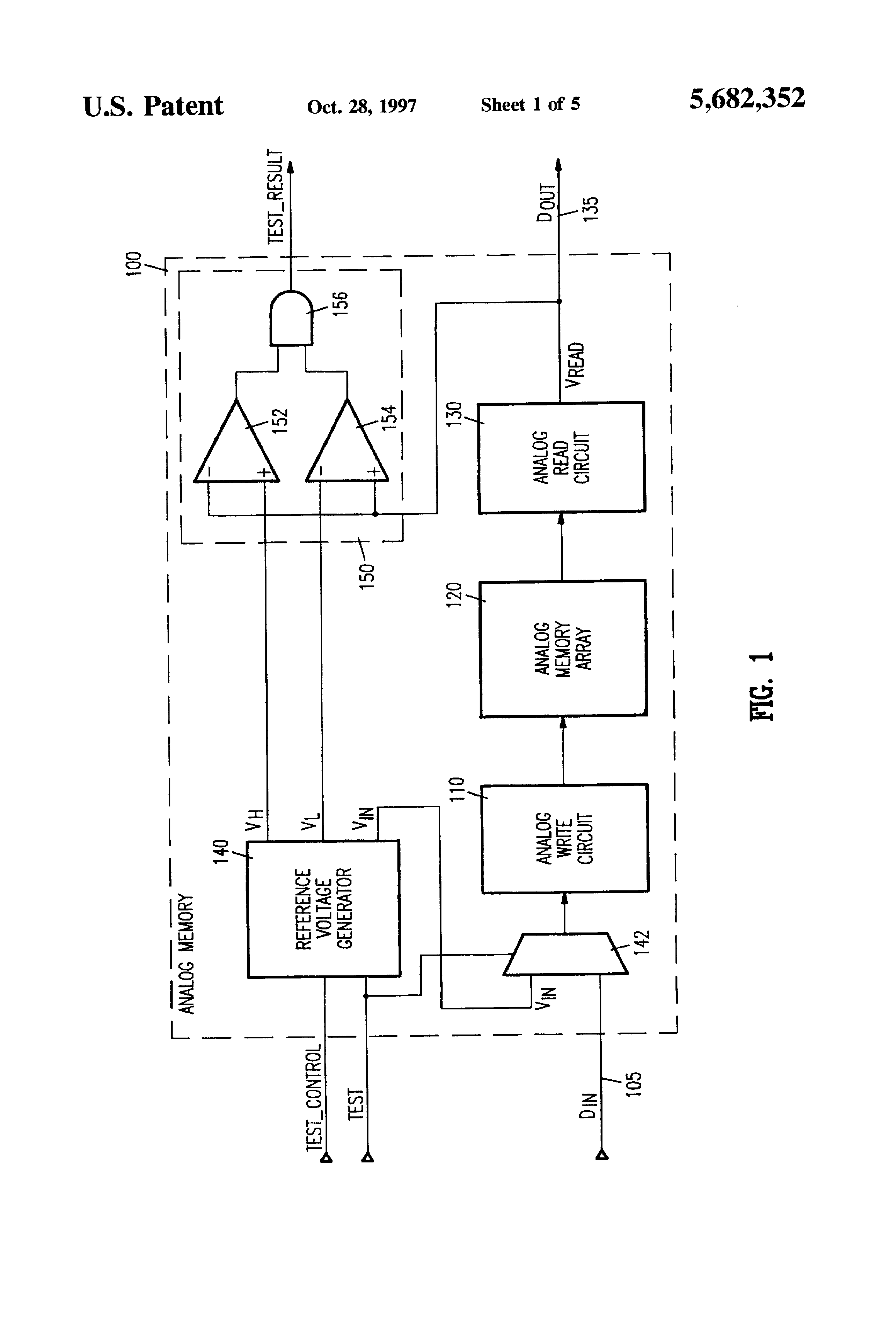
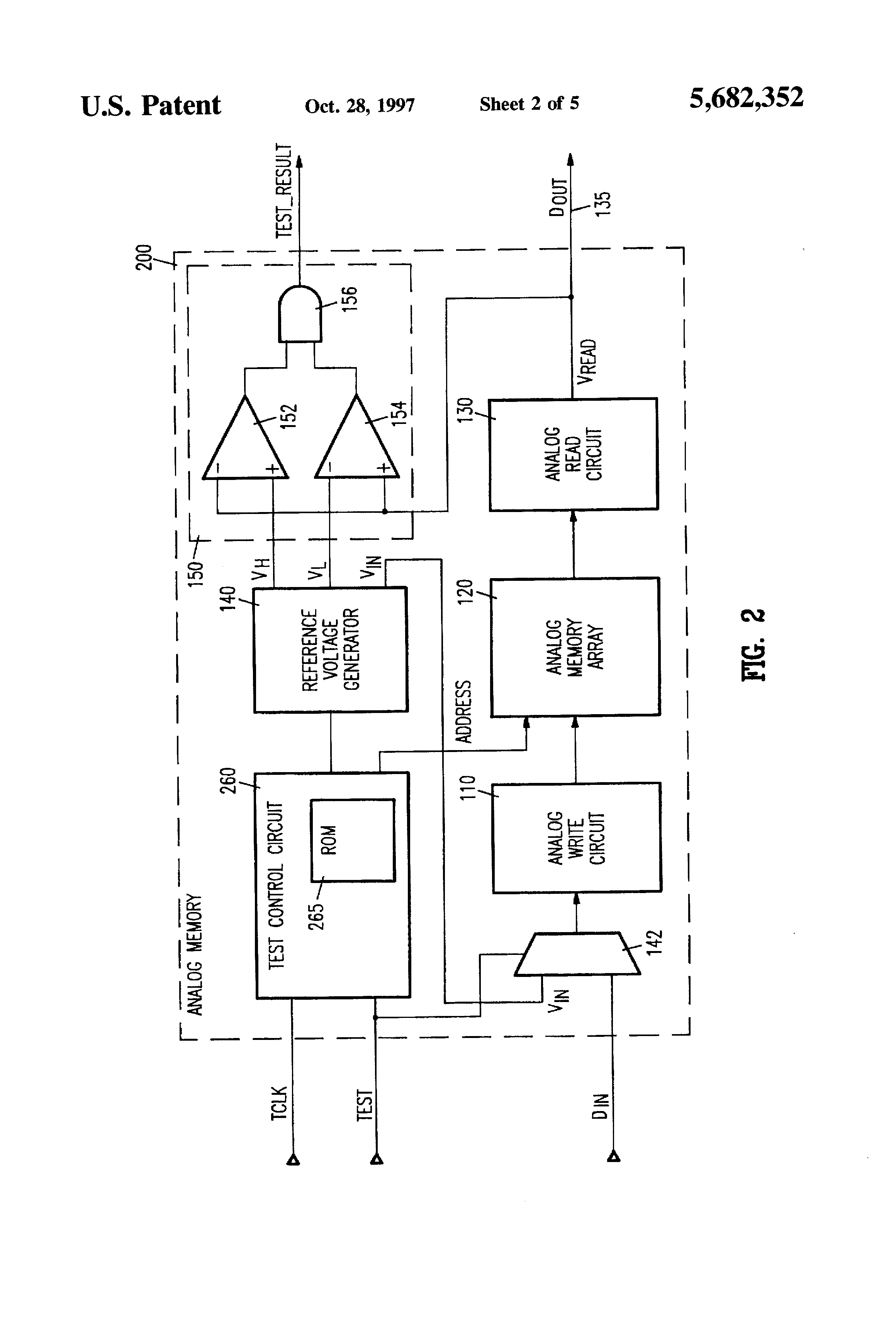
FIGS. 1 and 2 show block diagrams of analog memories containing test circuits in accordance with two embodiments of the invention.

FIGS. 3, 4, and 5 are circuit diagrams of on-chip resistor tree structures which provide intermediate voltages for testing an analog memory in accordance with different embodiments of the invention.

Use of the same reference symbols in different figures indicates similar or identical items.

DETAILED DESCRIPTION OF THE PREFERRED EMBODIMENTS

In accordance with an aspect of the invention, an analog integrated circuit (IC), i.e. an IC which manipulates analog input and/or output signals, contains on-chip test circuits for testing the analog functions of the analog IC. The on-chip test circuits implement analog functions internal to the analog IC but have only digital input and output signals. An external digital tester can control the on-chip test circuits by generating the required digital control signals and examining the digital result signals. Accordingly, expensive analog testers are not required for testing the analog IC during manufacture.

Pads used by digital test equipment to access the test circuits during manufacture can be made inaccessible to the user of the analog IC by not connecting the pads to output pins during packaging of the IC. In such embodiments of the invention, the addition of testing circuits does not increase the pin count of the analog IC. Alternatively, the test circuits can be user-accessible through separate pins for the test circuits or if low pin count is important, through multiplexed pins which connect to the test circuits when the chip is in a special test mode and connect to other circuits during normal chip functions. When the test circuits are user accessible, the user can test the analog IC in the application of the analog IC. User testing is particularly useful for non-volatile analog memory which, like conventional EPROM, EEPROM, and Flash memories, have write and read characteristics that may vary with the number of write/erase cycles performed throughout the memory's life.

In one embodiment of the invention, an on-chip test circuit includes a reference voltage generator and comparison logic. The reference voltage generator generates intermediate voltages at levels between digital "high" or "1" and "low" or "0" voltages. During testing, the intermediate voltages replace analog input signals required for testing the analog IC and/or provide references for the comparison logic. The comparison logic may, for example, include on-chip analog comparators which compare analog output signals to the internally generated intermediate voltages and produce a digital result signal.

FIG. 1 shows a block diagram of an integrated analog memory 100 which is a monolithic structure and may be fabricated using conventional semiconductor IC fabrication techniques. Analog memory IC 100 contains an analog write circuit 110, an analog memory array 120, and an analog read circuit 130 which may have any design capable of writing, storing, and reading analog values. U.S. patent application No. 08/333,381, entitled "High Resolution Analog Storage EPROM and Flash EPROM", which is hereby incorporated by reference herein in its entirety, describes suitable read circuits, write circuits, and memory cells for an embodiment of the invention where channel hot electron injection is used for writing analog values to non-volatile memory cells. Another embodiment of the invention employs EEPROM or Flash EEPROM and the Fowler-Nordheim tunneling (FNT) mechanism for writing analog values. Still other embodiments of the invention can employ other types of memory not restricted to non-volatile memory. For example, analog memory array 120 could be a volatile memory such as an analog DRAM array, where each memory cell contains a capacitor and an analog value is stored as a corresponding amount of charge in a memory cell's capacitor.

During a normal write to analog memory 100, an external source such as a microphone input (not shown) asserts an analog input signal DIN which passes through a multiplexer 142 to analog write circuit 110. The voltage level of signal DIN at a particular instant represents an analog sample or value to be written to a memory cell. Typically, digital address signals are required to select cells where values are written. The address signals may be generated internally (i.e. in analog memory 100) or externally (from outside analog memory 100). Analog write circuit 110 writes a value to a selected memory cell by changing a property such as the analog memory cell's threshold voltage to a state which indicates the value written. In such embodiments, the possible threshold voltages of an analog memory cell have a one-to-one relationship with the possible voltage levels of signal DIN. The values written to analog memory array 120 remain stored as long as the analog memory cells' states are preserved.

Analog read circuit 130 reads the analog values stored in analog memory array 120. Reading generates an analog output signal DOUT having a voltage level which indicates an analog value read from analog memory array 120. For proper operation of analog memory IC 100, the value read from a memory cell should equal the value written to the memory cell. Typically, this requires that the voltage level of output data signal DOUT during reading of a value be approximately equal to the voltage level of input data signal DIN when the value was written to analog memory array 120. Some error or difference is permitted between values read and values written because exact reproduction of analog values cannot be easily achieved and is generally not required.

A range of acceptable differences between values written and values read is sometimes referred to herein as the resolution of analog memory 100 because values which differ from each other by more than the resolution can be resolved or distinguished from each other but values which differ by less than the resolution may be indistinguishable from each other after being stored. During manufacture, each analog memory IC is tested to determine its resolution. The analog memory IC can be graded according to resolution or if the resolution is very poor, discarded as defective.

To facilitate resolution determination, analog memory IC 100 contains test circuits which allow digital testing of analog functions without external analog test equipment or circuits. In particular, analog memory IC 100 contains a reference voltage generator 140 and comparison logic 150. Reference voltage generator 140 generates voltages VIN, VL, and VH which have levels selected according to a digital control signal TEST-- CONTROL. Comparison logic 150 generates a digital test result signal TEST-- RESULT based on comparisons of analog output signal DOUT to voltages VL and VH from reference voltage generator 140.

Exemplary embodiments of reference voltage generator 140 which generate voltages VIN, VL, and VH at levels dictated by digital test control signal TEST-- CONTROL are described below in regard to FIGS. 3, 4, and 5. During testing, an enable signal TEST is asserted to reference voltage generator 140 and multiplexer 142. Signal TEST is the select signal for multiplexer 142 and causes multiplexer 142 to pass voltage VIN from reference voltage generator 140 to analog write circuit 110. Analog write circuit 110 may contain an input amplifier which amplifies an input analog signal from an external source, for example, so that the maximum voltage of the input signal corresponds to the maximum value that can be written to analog memory array 120. Voltage VIN can either be input to the input amplifier or can bypass the input amplifier. When voltage VIN bypasses the input amplifier, additional testing of the input amplifier may be required. In either case, analog write circuit 110 writes a value represented by voltage VIN to a memory cell selected according to an address signal generated either internally or externally.

After writing the value represented by voltage VIN to analog memory array 120, testing proceeds with analog read circuit 130 reading the memory cell to which the value was written. Ideally, the value read is exactly equal to the value written, but a difference between the value written and the value read are acceptable if the difference is less than a resolution desired for analog memory 100. The acceptable differences between the value written and the value read prescribe a relationship between analog output signal DOUT and voltage VIN. In a typical case, the relationship which identifies a value corresponding to an input voltage also identifies a value corresponding to an output voltage, and signal DOUT must be within a fixed voltage range of voltage VIN to meet the resolution requirements. In other cases, signal DOUT is proportional to voltage VIN or related to voltage VIN in some other fashion when the value read is exactly equal to the value written, and the acceptable voltage range for signal DOUT may not contain voltage VIN.

Voltages VL and VH are the boundaries of the acceptable voltage range for analog output signal DOUT. If read circuit 130 contains an output amplifier, signal DOUT can be taken from an input terminal or an output terminal of the output amplifier provided that voltages VL and VH are properly selected. Analog output signal DOUT and voltages VL and VH are input to comparison logic 150 which determines whether signal DOUT is between voltages VL and VH. In the typical case, voltage VL is less than voltage VIN by an amount ΔV, and voltage VH is greater than VIN by ΔV, where ΔV depends on the resolution being tested. For example, if the range of analog signal DOUT is 5 volts and the desired resolution provides the equivalent of eight bits of information (256 levels), ΔV must be less than about 10 mV.

Comparison logic 150 includes analog comparators 152 and 154 and an AND gate 156. Analog comparator 152 or 154 may be a differential amplifier or op-amp which generates a digital "high" output voltage if the voltage applied to a positive input terminal of the amplifier is greater than the voltage applied to a negative input terminal of the amplifier and generates a digital "low" output voltage if the voltage applied to the positive input terminal is less than the voltage applied to the negative input terminal. Accordingly, the output voltage from analog comparator 154 is high if analog output signal DOUT is greater than voltage VL, and the output voltage from analog comparator 152 is high if analog output signal DOUT is less than voltage VH. AND gate 156 asserts signal TEST-- RESULT high if analog signal DOUT is within the range greater than voltage VL but less than voltage VH.

To measure the resolution of analog memory 100, a digital test can change digital control signals so that a gap between voltages VH and VL incrementally decreases until test result signal indicates the signal read from the memory cell is outside the range from VL to VH or incrementally increases until test result signal indicates the signal read from the memory cell is within the range from VL to VH. The difference between VL and VH as indicated by the digital control signals when the value of the result signal changes indicates the resolution of the memory cell under test.

Testing can continue by allowing analog memory 100 to sit for a period of time then re-testing the memory cells to determine if any drift in the stored values has occurred. Alternatively or additionally, the memory cells which store data are re-tested after exposing analog memory 100 to high temperatures in a bake-in process and/or after applying stress voltages to the memory cells which store data. Accordingly, the testing simulates actual use of the analog memory.

After writing a value represented by a first voltage and testing a memory cell, a second value represented by a second voltage from reference voltage generator 140 can be written to the memory cell, and the resolution of the memory cell can then be tested in the vicinity of the second value. For a more complete testing of the memory cell, values near the bottom, middle, and top of the range which can be written to memory array 100 can be tested for resolution. If memory array 100 is a non-volatile memory, writing of each value can be preceded by an erase. Alternatively, it may be possible to write successive values without erasing if the values follow an order which successively increases the threshold voltage of a memory cell.

During the above described tests, an external tester only needs to supply digital signals such as signals TEST, TEST-- CONTROL, and address signals and only needs to examine digital signals such as signal TEST-- RESULT. Accordingly, an inexpensive digital tester can test the analog read and write processes of analog memory IC 100. Additionally, the test can be more accurate than those performed by analog testers because the analog signals (i.e. intermediate voltages) generated internally for testing of analog memory IC 100 are less susceptible to noise which may arise in leads of analog testers.

FIG. 2 shows an analog memory 200 in accordance with another embodiment of the invention. Analog memory 200 contains analog write circuit 110, analog memory array 120, analog read circuit 130, reference voltage generator 140, and comparison logic 150 such as described above in regard to FIG. 1. Analog memory 200 further includes a test control circuit 260 to reduce the number of external signals required for testing of analog memory 200. In particular, test control circuit 260, when activated by enable signal TEST, generates necessary test control signals to reference voltage generator 140 and/or address signals to analog memory array 120 as required to test the function of analog memory IC 200. Such signals may be from sequential addresses in a ROM 265. To test write and read functions of analog memory 200, an external tester asserts enable signal TEST and a clock signal TCLK to synchronize the sequence of address and control signals from test control circuit 260 with the tester. The tester then observes digital signal TEST-- RESULT to determine whether the analog functions work as desired.

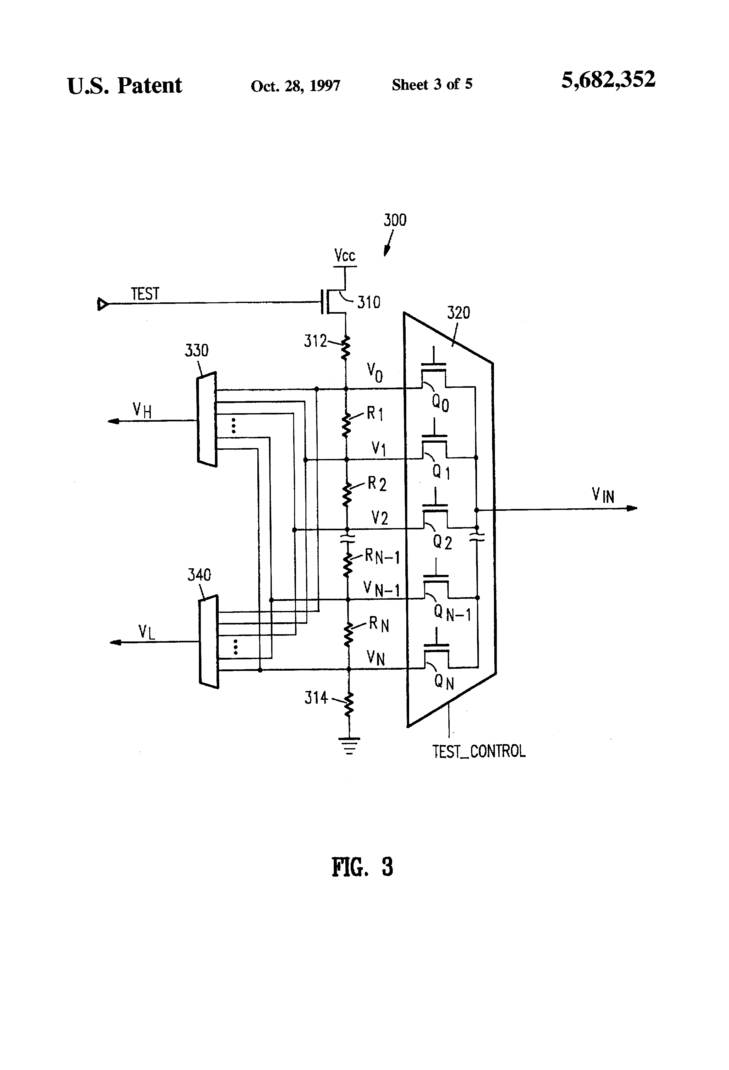
FIG. 3 shows an embodiment of a resistor tree structure 300 usable as reference voltage generator 140 in analog memory 100 (FIG. 1) or 200 (FIG. 2). Resistor tree structure 300 includes a transistor 310 and a set of resistors R1 to RN which are connected in series between a supply voltage Vcc and ground. Index N can be any desired integer. When enable signal TEST turns on a transistor 310, resistors R1 to RN act as a voltage divider, and a series of intermediate voltages V0 to VN develop at taps between resistors R1 to RN. Optionally, a resistor 312 and/or a resistor 314 can be added to the series of resistors to keep the highest intermediate voltage V0 below supply voltage Vcc and/or the lowest intermediate voltage VN above ground potential. A multiplexer 320 selects one of voltages V0 to VN as voltage VIN. Similarly, multiplexers 330 and 340 select voltages VH and VL, respectively.

In the embodiment of FIG. 3, multiplexer 320 is a collection of transistors Q0 to QN connected to taps in resistor tree structure 300, and control signal TEST-- CONTROL is a multi-bit digital signal which turns on at most one of transistors Q0 to QN to select one of voltages V0 to VN. Alternatively, any multiplexer design may be employed for multiplexers 320, 330, and 340.

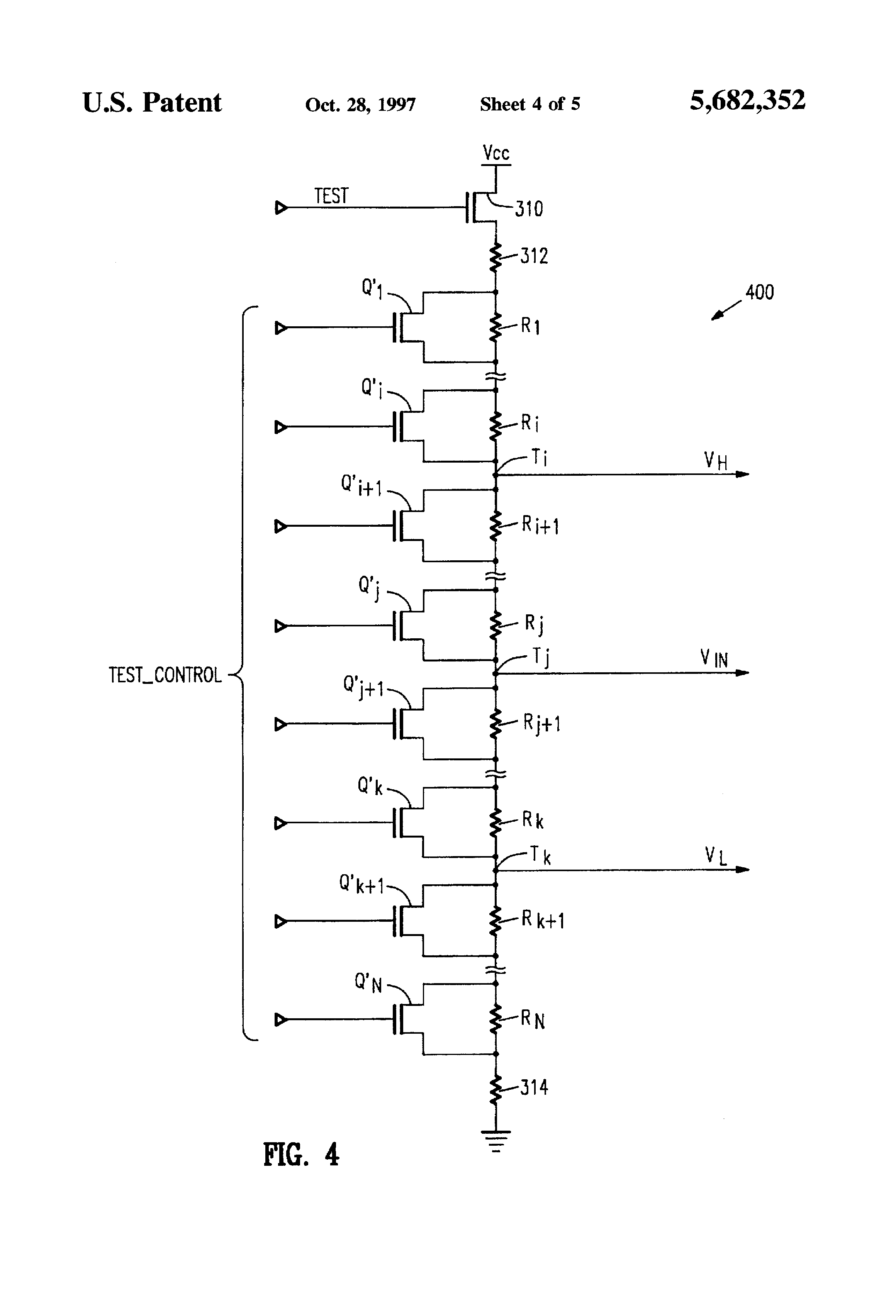
FIG. 4 shows another resistor tree structure 400 which is usable as reference voltage generator 140 in analog memory 100 or 200. Resistor tree structure 400 also contains a set of resistors R1 to RN which are connected in series; but in tree structure 400, each resistor R1 to RN is connected in parallel with a corresponding one of shunt transistors Q1 ' to QN ', and fixed taps Ti, Tj, and Tk supply voltages VH, VIN and VL. Signal TEST-- CONTROL selects levels for voltages VH, VIN and VL by turning on a desired set of shunt transistors Q1 ' to QN '. Each shunt transistor turned on creates a short across an associated resistor which increases the voltage level at taps between the transistor and ground and decreases the voltage at taps between the transistor and supply voltage Vcc. Voltage VIN is determined by the ratio of the effective resistance between tap Tj and supply voltage Vcc and the effective resistance between tap Tj and ground. Similarly, voltages VH and VL have levels determined by effective resistance above and below their respective source taps Ti and Tk.

In one embodiment of resistor tree structure 400, each of resistors R1 to RN has the same resistance. In an alternative embodiment, resistors R1 to RN have different resistances. For example, for each set of resistors such as R1 to Ri, Ri+1 to Rj, Rj+1 to Rk, and Rk+1 to RN, each resistor in the set can have twice the resistance of an adjacent resistor in the set. If the resistors in a set are related in this manner, the total resistance of the set is configurable in steps equal to the smallest resistance in the set. Alternatively, a nearly limitless number of other resistance combinations are possible.

FIG. 5 shows yet another resistor tree structure 500 which is usable as reference voltage generator 140 in analog memory 100 or 200. In tree structure 500, transistor 310 and resistors R1 to RN are connected in series between supply voltage Vcc and ground. A tap Tj, between resistors Rj and Rj+1, is the source of voltage VIN. Signal TEST-- CONTROL sets or changes voltage VIN by turning on desired ones of shunt transistors Q'1 to Q'i and Q'k+1 to Q'N which effects voltage VIN in the same manner as shunt transistors in resistor tree 400 of FIG. 4.

Multiplexer 530 selects one of taps Ti to Tj-1 as the source of voltage VH. Since taps Ti to Tj-1 are nearer supply voltage Vcc than is tap Tj, voltage VH is higher than voltage VIN. Multiplexer 540 selects one of taps Tj+1 to Tk as the source of voltage VL. Since taps Tj+1 to Tk are nearer ground than is tap Tj, voltage VL is lower than voltage VIN. If resistors Ri+1 to Rj are identical to resistors Rj+1 to Rk and the same select signals are applied to multiplexer 530 and multiplexer 540, the absolute difference ΔV between voltage VIN and VH will be equal to the absolute difference ΔV between voltage VIN and VL. Accordingly, for resistor tree 500, control signals to the shunt transistors Q'1 to Q'i and Q'k+1 to Q'N control the level of voltage VIN, and control signals to multiplexers 530 and 540 select ΔV (the resolution being tested).

Resistor trees 300, 400, and 500 are only examples of reference voltage generators in accordance with the invention. Various modification are possible. For example, separate resistor trees can provide one or more of voltages VIN, VH, and VL. Additionally, other circuits such as bandgap generators can generate required intermediate voltages, for example, when the absolute voltage levels are critical.

Although the invention has been described with reference to particular embodiments, the description is only an example of the invention's application and should not be taken as a limitation. For example, although a method for testing the resolution of an analog memory has been described, the same techniques can be used to test the accuracy of an analog output signal from any analog IC. Various other adaptations and combinations of features of the embodiments disclosed are within the scope of the present invention as defined by the following claims.
Claims (25)

  1. An integrated circuit comprising: an array of analog memory cells; an analog write circuit coupled to the array; an analog read circuit coupled to the array; an analog comparator having a first input terminal and a second input terminal, the analog comparator generating an output signal having a digital state indicating whether a first input voltage is greater than a second input voltage level, a first input terminal of the analog comparator being connected to an output terminal of the read circuit when the read circuit reads a test value from the analog memory array; and a reference voltage generator coupled to provide a first voltage to the analog write circuit during writing of the test value and a second voltage to a second input terminal of the analog comparator during reading of the test value, wherein the first voltage represents the test value.
  2. The integrated circuit of claim 1, wherein the first voltage and second voltage differ by an amount that depends on a desired resolution of the analog memory cells.
  3. The integrated circuit of claim 1, further comprising a second analog comparator which generates an output signal having a digital state indicating whether a first input voltage is greater than a second input voltage, wherein during reading of the test value from the memory array, a third voltage from the reference voltage generator is applied to a first input terminal of the second analog comparator and the output signal from the read circuit is applied to a second input terminal of the second analog comparator.
  4. The integrated circuit of claim 3, wherein the second voltage is greater than the first voltage, and the third voltage is less than the first voltage.
  5. The integrated circuit of claim 1, wherein the reference voltage generator comprises a resistor tree structure.
  6. The integrated circuit of claim 5, wherein the resistor tree structure comprises: a plurality of resistors connected in series, wherein a plurality of taps are between the resistors; and a first multiplexer having input terminals coupled to the plurality of taps.
  7. The integrated circuit of claim 6, further comprising a second multiplexer having input terminals coupled to the plurality of taps, wherein the first multiplexer selects one of the taps to supply the first voltage and the second multiplexer selects one of the taps to supply the second voltage.
  8. The integrated circuit of claim 5, wherein the resistor tree structure comprises: a plurality of resistors connected in series, wherein a plurality of taps are between the resistors; and a plurality of shunt transistors, each shunt transistor being connected in parallel with a corresponding one of the plurality of resistors.
  9. The integrated circuit of claim 8, wherein one of the plurality of taps supplies the first voltage.
  10. The integrated circuit of claim 9, further comprising a multiplexer coupled to a set of the taps, wherein the multiplexer selects one of the taps to supply the second voltage.
  11. The integrated circuit of claim 1, further comprising packaging which makes the reference voltage generator and the analog comparator inaccessible to a user of the integrated circuit.
  12. The integrated circuit of claim 1, further comprising packaging which makes the reference voltage generator and the analog comparator accessible to a user of the integrated circuit.
  13. An integrated circuit comprising: an array of analog memory cells; means for writing in the array a value represented by an analog input signal; means for reading the array to generate an analog output signal representing a value read from the array; and digitally operable test circuitry comprising: means for using the writing means to write a test value to the array; and means for generating a digital output signal indicating whether the analog output signal from the reading means accurately represents the test value.
  14. The integrated circuit of claim 13, wherein the digitally operable test circuitry further comprises: means for generating a first voltage and a second voltage, wherein the first voltage indicates to the writing means the test value for writing in the array; and means for generating a first signal having a digital state indicating whether the analog output signal has a voltage level grater than the second voltage.
  15. The integrated circuit of claim 14, further comprising: means for generating a third voltage; and means for generating a second signal having a digital state indicating whether the analog output signal has a voltage level less than the third voltage.
  16. The integrated circuit of claim 15, wherein the digital output signal has a digital state indicating whether the analog output signal has a voltage level greater than the second voltage and less than the third voltage.
  17. A method for testing an analog memory, comprising the steps of: providing resistor tree structure incorporated on-chip with the analog memory; writing to a selected memory cell in the analog memory a value represented by a first voltage from the resistor tree structure; reading the selected memory cell to generate an analog output signal representing a value read from the selected memory cell; comparing the analog output signal to a second voltage from the resistor tree structure; and generating a digital signal which indicates whether the analog output signal is at a voltage level greater than the second voltage.
  18. The method of claim 17, wherein the second voltage differs from the first voltage by an amount that depends on a desired resolution for the analog memory.
  19. The method of claim 17, further comprising: comparing the analog output signal to a third voltage from the resistor tree structure; and generating a digital result signal which indicates whether the output signal is at a voltage level between the second and third voltages.
  20. The method of claim 19, wherein a voltage difference between the second voltage and the first voltage is equal to a voltage difference between the third voltage and the first voltage.
  21. The method of claim 19, further comprising: varying the second and third voltage levels systematically until the digital result signal changes; and determining the resolution of the analog memory from the second and third voltages which causes the digital result signal to change.
  22. The method of claim 19, further comprising: writing to the selected memory cell a second value represented by a fourth voltage from the resistor tree structure; reading the selected memory cell to generate a second analog output signal; comparing the second analog output signal to a fifth voltage and a sixth voltage from the resistor tree structure; and generating a digital result signal which indicates whether the second analog output signal is at a voltage level between the fifth and sixth voltages.
  23. The method of claim 17, wherein comparing the output signal to the second voltage comprises: applying the output signal to a first input terminal of a first analog comparator which is incorporated on-chip with the analog memory; and applying the second voltage to a second input terminal of the first analog comparator, wherein the first analog comparator generates the digital signal which indicates whether the analog output signal is at a voltage level greater than the second voltage.
  24. The method of claim 23, further comprising: applying a third voltage from the resistor tree structure to a first input terminal of a second analog comparator which is incorporated on-chip with the analog memory; applying the analog output signal to a second input terminal of the second analog comparator, wherein the second analog comparator generates a digital signal which indicates whether the analog output signal is at a voltage level less than the third voltage; and applying the digital signals from the first and second analog comparators to an AND gate to generate a digital result signal that indicates whether the analog output signal is greater than the second voltage and less than the third voltage.
  25. An integrated circuit comprising: analog circuitry which generates an analog output signal from an analog input signal; a reference voltage generator coupled to the analog circuitry, the reference voltage generator generating a first intermediate voltage, a second intermediate voltage, and a third intermediate voltage, wherein during testing of the analog circuitry, the reference voltage generator provides to the analog circuitry the first intermediate voltage in place of the analog input signal; a first analog comparator coupled to the analog circuitry and the reference voltage generator, wherein during testing of the analog circuitry, the first analog comparator generates a first digital signal indicating whether the analog output signal from the analog circuitry is greater than the second intermediate voltage; a second analog comparator coupled to the analog circuitry and the reference voltage generator, wherein during testing of the analog circuitry, the second analog comparator generates a second digital signal indicating whether the analog output signal from the analog circuitry is less than the third intermediate voltage; and a gate coupled to generate a digital result signal which is a logical AND of the first and second digital signals.

Publications

Related applications (3)

  1. US08/598,485

    Priority application

  2. US08/598,485

    Claims priority

  3. US08/598,485

    Patent family

Record timeline

  1. Application filed by Invoice Technology Inc

  2. Priority to US08/598,485

  3. Assigned to INVOICE TECHNOLOGY, INC.

  4. Application granted

  5. Publication of US5682352A

  6. Assigned to INVOX TECHNOLOGY

  7. Assigned to SANDISK CORPORATION

  8. Assigned to SANDISK TECHNOLOGIES INC.

  9. Anticipated expiration

  10. Assigned to SANDISK TECHNOLOGIES LLC

  11. Expired - LifetimeCurrent

Legal events

  1. AS

    Assignment

    Owner name: INVOICE TECHNOLOGY, INC., CALIFORNIA

    Free format text: ASSIGNMENT OF ASSIGNORS INTEREST;ASSIGNORS:WONG, SAU C.;SO, HOCK C.;REEL/FRAME:007885/0153

    Effective date: 19960207

  2. AS

    Assignment

    Owner name: INVOX TECHNOLOGY, CALIFORNIA

    Free format text: CHANGE OF NAME;ASSIGNOR:INVOICE TECHNOLOGY, INC.;REEL/FRAME:009436/0618

    Effective date: 19970623

  3. AS

    Assignment

    Owner name: SANDISK CORPORATION, CALIFORNIA

    Free format text: ASSIGNMENT OF ASSIGNORS INTEREST;ASSIGNOR:INVOX TECHNOLOGY;REEL/FRAME:011812/0888

    Effective date: 19990920

  4. REMI

    Maintenance fee reminder mailed

  5. FEPP

    Fee payment procedure

    Free format text: PETITION RELATED TO MAINTENANCE FEES FILED (ORIGINAL EVENT CODE: PMFP); ENTITY STATUS OF PATENT OWNER: LARGE ENTITY

  6. FEPP

    Fee payment procedure

    Free format text: PETITION RELATED TO MAINTENANCE FEES GRANTED (ORIGINAL EVENT CODE: PMFG); ENTITY STATUS OF PATENT OWNER: LARGE ENTITY

  7. FP

    Lapsed due to failure to pay maintenance fee

    Effective date: 20011028

  8. FPAY

    Fee payment

    Year of fee payment: 4

  9. STCF

    Information on status: patent grant

    Free format text: PATENTED CASE

  10. SULP

    Surcharge for late payment

  11. PRDP

    Patent reinstated due to the acceptance of a late maintenance fee

    Effective date: 20020701

  12. FPAY

    Fee payment

    Year of fee payment: 8

  13. FPAY

    Fee payment

    Year of fee payment: 12

  14. AS

    Assignment

    Owner name: SANDISK TECHNOLOGIES INC., TEXAS

    Free format text: ASSIGNMENT OF ASSIGNORS INTEREST;ASSIGNOR:SANDISK CORPORATION;REEL/FRAME:026224/0055

    Effective date: 20110404

  15. AS

    Assignment

    Owner name: SANDISK TECHNOLOGIES LLC, TEXAS

    Free format text: CHANGE OF NAME;ASSIGNOR:SANDISK TECHNOLOGIES INC;REEL/FRAME:038807/0980

    Effective date: 20160516

Patent citations (4)

  1. US5163021A

    Multi-state EEprom read and write circuits and techniques

    Sundisk Corporation · November 10, 1992 · Examiner cited

  2. US5481551A

    IC element testing device

    Fujitsu Limited · January 2, 1996 · Examiner cited

  3. US5539699A

    Flash memory testing apparatus

    Advantest Corporation · July 23, 1996 · Examiner cited

  4. US5528603A

    Apparatus and method for testing an integrated circuit using a voltage reference potential and a reference integrated circuit

    Micron Technology, Inc. · June 18, 1996 · Examiner cited

Cited by (108)

  1. US6330185B1

    High bandwidth multi-level flash memory using dummy memory accesses to improve precision when writing or reading a data stream

    Multi Level Memory Technology · December 11, 2001

  2. US6278633B1

    High bandwidth flash memory that selects programming parameters according to measurements of previous programming operations

    Multi Level Memory Technology · August 21, 2001

  3. US6363008B1

    Multi-bit-cell non-volatile memory with maximized data capacity

    Multi Level Memory Technology · March 26, 2002

  4. US6558967B1

    Multi-bit-per-cell memory system with numbers of bits per cell set by testing of memory units

    Multi Level Memory Technology · May 6, 2003

  5. US7079422B1

    Periodic refresh operations for non-volatile multiple-bit-per-cell memory

    Samsung Electronics Co., Ltd. · July 18, 2006

  6. US6396744B1

    Flash memory with dynamic refresh

    Multi Level Memory Technology · May 28, 2002

  7. US6522586B2

    Dynamic refresh that changes the physical storage locations of data in flash memory

    Multi Level Memory Technology · February 18, 2003

  8. US6754128B2

    Non-volatile memory operations that change a mapping between physical and logical addresses when restoring data

    Multi Level Memory Technology · June 22, 2004

  9. US6856568B1

    Refresh operations that change address mappings in a non-volatile memory

    Multi Level Memory Technology · February 15, 2005

  10. WO2002014883A3

    Analog signal testing circuit and -method

    Xilinx Inc · May 16, 2002 · Examiner cited

  11. US6653827B2

    Analog signal test circuit and method

    Xilinx, Inc. · November 25, 2003

  12. WO2002033557A3

    Single-source or single-destination signal routing

    Motorola Inc · August 22, 2002 · Examiner cited

  13. US6961881B2

    Semiconductor device

    Fujitsu Limited · November 1, 2005 · Examiner cited

  14. US20060015788A1

    Semiconductor device

    Fujitsu Limited · January 19, 2006 · Examiner cited

  15. EP1293989A3

    Test method for semiconductor memory circuit

    Fujitsu Limited · January 3, 2007 · Examiner cited

  16. US7243274B2

    Semiconductor device

    Fujitsu Limited · July 10, 2007

  17. US20030065997A1

    Semiconductor device

    Fujitsu Limited · April 3, 2003 · Examiner cited

  18. EP1890298A1

    Test method for semiconductor memory circuit

    Fujitsu Ltd. · February 20, 2008 · Examiner cited

  19. EP1890297A1

    Test method for semiconductor memory circuit

    Fujitsu Ltd. · February 20, 2008 · Examiner cited

  20. US7088172B1

    Configurable voltage bias circuit for controlling buffer delays

    Xilinx, Inc. · August 8, 2006 · Examiner cited

  21. US7321482B2

    Sub-circuit voltage manipulation

    Hewlett-Packard Development Company, L.P. · January 22, 2008

  22. US7447066B2

    Memory with retargetable memory cell redundancy

    Sandisk Corporation · November 4, 2008

  23. US20070103978A1

    Memory with retargetable memory cell redundancy

    Conley Kevin M · May 10, 2007 · Examiner cited

  24. US20070103977A1

    Retargetable memory cell redundancy methods

    Conley Kevin M · May 10, 2007 · Examiner cited

  25. US7379330B2

    Retargetable memory cell redundancy methods

    Sandisk Corporation · May 27, 2008

  26. US7307468B1

    Bandgap system with tunable temperature coefficient of the output voltage

    Xilinx, Inc. · December 11, 2007

  27. US8156403B2

    Combined distortion estimation and error correction coding for memory devices

    Anobit Technologies Ltd. · April 10, 2012

  28. US20080198650A1

    Distortion Estimation And Cancellation In Memory Devices

    Anobit Technologies Ltd. · August 21, 2008 · Examiner cited

  29. US8050086B2

    Distortion estimation and cancellation in memory devices

    Anobit Technologies Ltd. · November 1, 2011

  30. US8599611B2

    Distortion estimation and cancellation in memory devices

    Apple Inc. · December 3, 2013

  31. US8570804B2

    Distortion estimation and cancellation in memory devices

    Apple Inc. · October 29, 2013

  32. US8239735B2

    Memory Device with adaptive capacity

    Apple Inc. · August 7, 2012

  33. US8060806B2

    Estimation of non-linear distortion in memory devices

    Anobit Technologies Ltd. · November 15, 2011

  34. US20100131826A1

    Estimation of non-linear distortion in memory devices

    Anobit Technologies Ltd. · May 27, 2010 · Examiner cited

  35. US20100165730A1

    Reading memory cells using multiple thresholds

    Anobit Technologies Ltd. · July 1, 2010 · Examiner cited

  36. USRE46346E1

    Reading memory cells using multiple thresholds

    Apple Inc. · March 21, 2017

  37. US8145984B2

    Reading memory cells using multiple thresholds

    Anobit Technologies Ltd. · March 27, 2012

  38. US7975192B2

    Reading memory cells using multiple thresholds

    Anobit Technologies Ltd. · July 5, 2011 · Examiner cited

  39. US7924648B2

    Memory power and performance management

    Anobit Technologies Ltd. · April 12, 2011

  40. US20080126686A1

    Memory power and performance management

    Anobit Technologies Ltd. · May 29, 2008 · Examiner cited

  41. US8151163B2

    Automatic defect management in memory devices

    Anobit Technologies Ltd. · April 3, 2012

  42. US20080133984A1

    Method for Inspecting the Electrical Performance of a Flash Memory Cell

    Semiconductor Manufacturing International (Shanghai) Corporation · June 5, 2008 · Examiner cited

  43. US7940584B2

    Method for inspecting the electrical performance of a flash memory cell

    Semiconductor Manufacturing International (Shanghai) Corporation · May 10, 2011 · Examiner cited

  44. US8151166B2

    Reduction of back pattern dependency effects in memory devices

    Anobit Technologies Ltd. · April 3, 2012

  45. US8369141B2

    Adaptive estimation of memory cell read thresholds

    Apple Inc. · February 5, 2013

  46. US8001320B2

    Command interface for memory devices

    Anobit Technologies Ltd. · August 16, 2011

  47. US20100131827A1

    Memory device with internal signap processing unit

    Anobit Technologies Ltd · May 27, 2010 · Examiner cited

  48. US8429493B2

    Memory device with internal signap processing unit

    Apple Inc. · April 23, 2013

  49. US8234545B2

    Data storage with incremental redundancy

    Apple Inc. · July 31, 2012

  50. US7925936B1

    Memory device with non-uniform programming levels

    Anobit Technologies Ltd. · April 12, 2011

  51. US8259497B2

    Programming schemes for multi-level analog memory cells

    Apple Inc. · September 4, 2012

  52. US20090043951A1

    Programming schemes for multi-level analog memory cells

    Anobit Technologies Ltd. · February 12, 2009 · Examiner cited

  53. US8174905B2

    Programming orders for reducing distortion in arrays of multi-level analog memory cells

    Anobit Technologies Ltd. · May 8, 2012

  54. US8527819B2

    Data storage in analog memory cell arrays having erase failures

    Apple Inc. · September 3, 2013

  55. US8068360B2

    Reading analog memory cells using built-in multi-threshold commands

    Anobit Technologies Ltd. · November 29, 2011

  56. US8000141B1

    Compensation for voltage drifts in analog memory cells

    Anobit Technologies Ltd. · August 16, 2011

  57. US8270246B2

    Optimized selection of memory chips in multi-chips memory devices

    Apple Inc. · September 18, 2012

  58. US8225181B2

    Efficient re-read operations from memory devices

    Apple Inc. · July 17, 2012

  59. US20090144600A1

    Efficient re-read operations from memory devices

    Anobit Technologies Ltd · June 4, 2009 · Examiner cited

  60. US8209588B2

    Efficient interference cancellation in analog memory cell arrays

    Anobit Technologies Ltd. · June 26, 2012

  61. US20090157964A1

    Efficient data storage in multi-plane memory devices

    Anobit Technologies Ltd. · June 18, 2009 · Examiner cited

  62. US8085586B2

    Wear level estimation in analog memory cells

    Anobit Technologies Ltd. · December 27, 2011

  63. US8156398B2

    Parameter estimation based on error correction code parity check equations

    Anobit Technologies Ltd. · April 10, 2012

  64. US7924587B2

    Programming of analog memory cells using a single programming pulse per state transition

    Anobit Technologies Ltd. · April 12, 2011

  65. US8230300B2

    Efficient readout from analog memory cells using data compression

    Apple Inc. · July 24, 2012

  66. US8400858B2

    Memory device with reduced sense time readout

    Apple Inc. · March 19, 2013

  67. US8059457B2

    Memory device with multiple-accuracy read commands

    Anobit Technologies Ltd. · November 15, 2011

  68. US7924613B1

    Data storage in analog memory cells with protection against programming interruption

    Anobit Technologies Ltd. · April 12, 2011

  69. US8498151B1

    Data storage in analog memory cells using modified pass voltages

    Apple Inc. · July 30, 2013

  70. US7995388B1

    Data storage using modified voltages

    Anobit Technologies Ltd. · August 9, 2011

  71. US8169825B1

    Reliable data storage in analog memory cells subjected to long retention periods

    Anobit Technologies Ltd. · May 1, 2012

  72. US8949684B1

    Segmented data storage

    Apple Inc. · February 3, 2015

  73. US8482978B1

    Estimation of memory cell read thresholds by sampling inside programming level distribution intervals

    Apple Inc. · July 9, 2013

  74. US8000135B1

    Estimation of memory cell read thresholds by sampling inside programming level distribution intervals

    Anobit Technologies Ltd. · August 16, 2011

  75. US8239734B1

    Efficient data storage in storage device arrays

    Apple Inc. · August 7, 2012

  76. US8261159B1

    Data scrambling schemes for memory devices

    Apple, Inc. · September 4, 2012

  77. US8713330B1

    Data scrambling in memory devices

    Apple Inc. · April 29, 2014

  78. US8208304B2

    Storage at M bits/cell density in N bits/cell analog memory cell devices, M>N

    Anobit Technologies Ltd. · June 26, 2012

  79. US8174857B1

    Efficient readout schemes for analog memory cell devices using multiple read threshold sets

    Anobit Technologies Ltd. · May 8, 2012

  80. US8397131B1

    Efficient readout schemes for analog memory cell devices

    Apple Inc. · March 12, 2013

  81. US8248831B2

    Rejuvenation of analog memory cells

    Apple Inc. · August 21, 2012

  82. US8924661B1

    Memory system including a controller and processors associated with memory devices

    Apple Inc. · December 30, 2014

  83. US20100220509A1

    Selective Activation of Programming Schemes in Analog Memory Cell Arrays

    Anobit Technologies Ltd · September 2, 2010 · Examiner cited

  84. US8228701B2

    Selective activation of programming schemes in analog memory cell arrays

    Apple Inc. · July 24, 2012

  85. US8832354B2

    Use of host system resources by memory controller

    Apple Inc. · September 9, 2014

  86. US8259506B1

    Database of memory read thresholds

    Apple Inc. · September 4, 2012

  87. US8238157B1

    Selective re-programming of analog memory cells

    Apple Inc. · August 7, 2012

  88. US8479080B1

    Adaptive over-provisioning in memory systems

    Apple Inc. · July 2, 2013

  89. US8495465B1

    Error correction coding over multiple memory pages

    Apple Inc. · July 23, 2013

  90. US8677054B1

    Memory management schemes for non-volatile memory devices

    Apple Inc. · March 18, 2014

  91. US8694814B1

    Reuse of host hibernation storage space by memory controller

    Apple Inc. · April 8, 2014

  92. US8572311B1

    Redundant data storage in multi-die memory systems

    Apple Inc. · October 29, 2013

  93. US8677203B1

    Redundant data storage schemes for multi-die memory systems

    Apple Inc. · March 18, 2014

  94. US8694853B1

    Read commands for reading interfering memory cells

    Apple Inc. · April 8, 2014

  95. US8572423B1

    Reducing peak current in memory systems

    Apple Inc. · October 29, 2013

  96. US8595591B1

    Interference-aware assignment of programming levels in analog memory cells

    Apple Inc. · November 26, 2013

  97. US9104580B1

    Cache memory for hybrid disk drives

    Apple Inc. · August 11, 2015

  98. US8767459B1

    Data storage in analog memory cells across word lines using a non-integer number of bits per cell

    Apple Inc. · July 1, 2014

  99. US8645794B1

    Data storage in analog memory cells using a non-integer number of bits per cell

    Apple Inc. · February 4, 2014

  100. US8856475B1

    Efficient selection of memory blocks for compaction

    Apple Inc. · October 7, 2014

  101. US8493781B1

    Interference mitigation using individual word line erasure operations

    Apple Inc. · July 23, 2013

  102. US8694854B1

    Read threshold setting based on soft readout statistics

    Apple Inc. · April 8, 2014

  103. US9021181B1

    Memory management for unifying memory cell conditions by using maximum time intervals

    Apple Inc. · April 28, 2015

  104. US11556416B2

    Controlling memory readout reliability and throughput by adjusting distance between read thresholds

    Apple Inc. · January 17, 2023

  105. US11847342B2

    Efficient transfer of hard data and confidence levels in reading a nonvolatile memory

    Apple Inc. · December 19, 2023

  106. CN114280460A

    Electrical test analog circuit

    上海安路信息科技股份有限公司 · April 5, 2022 · Examiner cited

  107. CN114705973A

    Non-invasive complex environment integrated circuit aging monitoring method

    北京航空航天大学杭州创新研究院 · July 5, 2022 · Examiner cited

  108. CN114705973B

    A non-invasive method for monitoring the aging of integrated circuits in complex environments

    北京航空航天大学杭州创新研究院 · November 11, 2022 · Examiner cited

Related Patents