Skip to content

Patent drawings

Drawing 1 of 4

US 4,774,421

Drawing 1 of 4

Expanded drawing 1 of 4 from US 4,774,421, Programmable logic array device using EPROM technology
High-resolution patent drawing

US 4,774,421

Programmable logic array device using EPROM technology

Filed
September 12, 1986
Granted
September 27, 1988
Assignee
Altera
Inventors
Robert F. Hartmann, Sau-Ching Wong, Yiu-Fai Chan, Jung-Hsing Ou

Abstract

A programmable logic array device basically comprising a programmable AND gate array (FIGS. 5, 11) having addressable rows (40-45) and columns (32-38) or memory cells (30, 31) which can be individually programmed to represent logic data; an input signal receiving circuit (FIG. 9) for developing a corresponding buffered input signal; a first row driver (FIG. 10) responsive to the buffered signal and operative to cause a particular row of memory cells in an AND array (FIG. 11) to output corresponding logical product of AND-input signals, OR/NOR sensing circuitry (FIG. 12) for sensing the AND array product signals and for developing therefrom corresponding logical OR sum signals; circuit means output terminal circuitry; output switching circuitry (FIG. 14) responsive to a control signal and operative to couple either the circuit means output signal or a registered (FIG. 13) output to a device input or output terminal (FIG. 16); feedback switching circuitry similarly responsive to a control signal and operative to couple either the circuit means output signal, registered output signal, or feedback signal to a row driver; and Reprogrammable Architecture control circuitry (FIG. 24) to provide control signals to said switching circuitry. The device has the advantages of increased density of useable logic functions, and decreased power consumption.

View on Google Patents ↗
View Full PatentComplete archived record · 4 figures · 149 description paragraphs · 27 claims

Patent record

Source
Google Patents
Publication
US4774421A
Application
US06/907,075
Priority
May 3, 1984
Prior art date
May 3, 1984
Publication date
September 27, 1988
Legal status
Expired - Lifetime
Original assignee
Altera Corp
Current assignee
Altera Corp
Prior art keywords
signal, input, output signal, logic, memory device
Source retrieved
July 20, 2026

Classifications

  • HELECTRICITY
  • H03ELECTRONIC CIRCUITRY
  • H03KPULSE TECHNIQUE
  • H03K17/00Electronic switching or gating, i.e. not by contact-making and –breaking
  • H03K17/51Electronic switching or gating, i.e. not by contact-making and –breaking characterised by the components used
  • H03K17/56Electronic switching or gating, i.e. not by contact-making and –breaking characterised by the components used by the use, as active elements, of semiconductor devices
  • H03K17/687Electronic switching or gating, i.e. not by contact-making and –breaking characterised by the components used by the use, as active elements, of semiconductor devices the devices being field-effect transistors
  • H03K17/693Switching arrangements with several input- or output-terminals, e.g. multiplexers, distributors
  • H03K19/00Logic circuits, i.e. having at least two inputs acting on one output; Inverting circuits
  • H03K19/02Logic circuits, i.e. having at least two inputs acting on one output; Inverting circuits using specified components
  • H03K19/08Logic circuits, i.e. having at least two inputs acting on one output; Inverting circuits using specified components using semiconductor devices
  • H03K19/094Logic circuits, i.e. having at least two inputs acting on one output; Inverting circuits using specified components using semiconductor devices using field-effect transistors
  • H03K19/09425Multistate logic
  • H03K19/173Logic circuits, i.e. having at least two inputs acting on one output; Inverting circuits using specified components using elementary logic circuits as components
  • H03K19/1733Controllable logic circuits
  • H03K19/1735Controllable logic circuits by wiring, e.g. uncommitted logic arrays
  • H03K19/1736Controllable logic circuits by wiring, e.g. uncommitted logic arrays in which the wiring can be modified
  • H03K19/1737Controllable logic circuits using multiplexers
  • H03K19/177Logic circuits, i.e. having at least two inputs acting on one output; Inverting circuits using specified components using elementary logic circuits as components arranged in matrix form
  • H03K19/17704Logic circuits, i.e. having at least two inputs acting on one output; Inverting circuits using specified components using elementary logic circuits as components arranged in matrix form the logic functions being realised by the interconnection of rows and columns
  • H03K19/17708Logic circuits, i.e. having at least two inputs acting on one output; Inverting circuits using specified components using elementary logic circuits as components arranged in matrix form the logic functions being realised by the interconnection of rows and columns using an AND matrix followed by an OR matrix, i.e. programmable logic arrays
  • H03K19/17712Logic circuits, i.e. having at least two inputs acting on one output; Inverting circuits using specified components using elementary logic circuits as components arranged in matrix form the logic functions being realised by the interconnection of rows and columns using an AND matrix followed by an OR matrix, i.e. programmable logic arrays one of the matrices at least being reprogrammable
  • H03K5/00Manipulating of pulses not covered by one of the other main groups of this subclass
  • H03K5/01Shaping pulses
  • H03K5/02Shaping pulses by amplifying
  • H03K5/023Shaping pulses by amplifying using field effect transistors

Figures

4 plates

Figure 1 of 4 from US 4,774,421, Programmable logic array device using EPROM technology
Figure 01Full resolution ↗
Figure 2 of 4 from US 4,774,421, Programmable logic array device using EPROM technology
Figure 02Full resolution ↗
Figure 3 of 4 from US 4,774,421, Programmable logic array device using EPROM technology
Figure 03Full resolution ↗
Figure 4 of 4 from US 4,774,421, Programmable logic array device using EPROM technology
Figure 04Full resolution ↗

Description

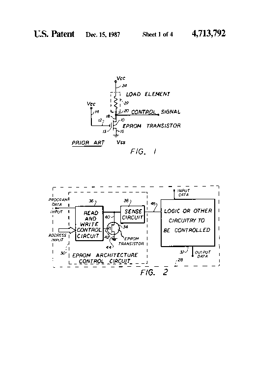
This application is a continuation of U.S. patent application Ser. No. 607,018 filed May 3, 1984, and is related to a copending application entitled "Programmable Logic Array Device Using EPROM Technology", now U.S. Pat. No. 4,609,986 issued Sept. 2, 1986, and a copending application, Ser. No. 742,089 filed June 6, 1985 and entitled "A Programmable Macro Cell Using EPROM or EEPROM Transistors for Architecture Control in Programmable Logic Circuits" now U.S. Pat. No. 4,713,792 issued Dec. 15, 1987, both of which are assigned to the assignee of the present invention.

BACKGROUND OF THE INVENTION

1. Field of the Invention

The present invention relates generaly to programmable logic array devices and more particularly to an erasable, electrically programmable logic device made using CMOS EPROM Floating Gate technology.

2. Discussion of the Technology and Prior Art

The integrated circuit technology used in the fabrication of the present invention is CMOS Floating Gate (CMOS EPROM). Floating gate technology allows "programming" of certain transistors such that when normal operating voltages are applied (0 to 5 volts) the "programmed" transistor acts like an open circuit. In their unprogrammed state, these same transistors will conduct when 5 volts is applied to the gate terminal and will appear as an open circuit when 0 volts is applied to the gate terminal.

In the past, the normal application of the technology was to manufacture electrically programmable read only memories (EPROM). The programmable element in EPROM technology is a two layer polysilicon MOS transistor. By changing the circuits which access the array of programmable elements, programmable logic arrays (PLA) can be realized. Prior art U.S. patents include: Kahng, U.S. Pat. No. 3,500,142, Frohman-Bentchkowsky, U.S. Pat. No. 3,660,819; Frohman-Bentchkowsky, U.S. Pat. No. 3,728,695; Frohman-Bentchkowsky, U.S. Pat. No. 3,744,036; Frohman-Bentchkowsky, U.S. Pat. No. 3,755,721; Frohman-Bentchkowsky, U.S. Pat. No. 3,825,946; Simko et al, U.S. Pat. No. 3,984,822; and Lohstroh et al, U.S. Pat. No. 4,019,197.

Programmable logic arrays and similar circuit elements such as programmable array logic (PAL) of the type disclosed in the U.S. Patent to Birkner et al, U.S. Pat. No. 4,124,899 (R) have been in existence for many years. See for example, the U.S. Patents to: Crawford et al, U.S. Pat. No. 3,541,543; Spenser, Jr., U.S. Pat. No. 3,566,153; Proebsting, U.S. Pat. No. 3,702,985; Greer, U.S. Pat. No. 3,816,725; Greer, U.S. Pat. No. 3,818,452; Greer, U.S. Pat. No. 3,849,638. The first realizations were mask programmed. An example is a P channel MOS device manufactured by Texas Instruments during 1968-1970.

More recently, the technology of choice has been fuse programmable bipolar technology made by manufacturers such as Signetics, Monolithic Memories, Inc., Advanced Micro Devices, Harris Semiconductor and others.

The complexity of PLAs and PALs is given in terms of:

(a) The number of Inputs;

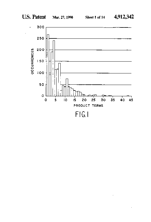
(b) The number of Product Terms in the AND array;

(c) The number of Sum Terms in the OR array;

(d) The number of Storage Elements (Flip Flops);

(e) The number of Feedback lines from the output of the OR array (or the Flip Flops) to the AND array; and

(f) The number of Outputs.

SUMMARY OF THE PRESENT INVENTION

The present invention relates to an electrically programmable integrated circuit with a logic complexity of approximately 300 (2-input) NAND gates. The preferred embodiment is designated The Altera EP300 and can generally be classed as a programmable logic array (PLA) with substantial additional circuitry such that many combinations of inputs, outputs and feedback can be accommodated.

The EP300 has the following characteristics:

(a) 10 Inputs (from off chip) to the AND array;

(b) 74 Product Terms (P-Terms);

(c) 8 Sum Terms (Fixed OR Structure with 8 P-Terms each);

(d) 8 D type Flip Flops;

(e) 8 Feedback lines; and

(f) 8 Outputs.

In addition to the above there are several other features of the EP300. These are listed below:

(a) One of the inputs (Pin #1) to the AND array also serves as the CLOCK to the D Flip Flops;

(b) The P-Terms are grouped as follows:

(1) 8 each to 8 fixed OR/NOR gates (64 P-Terms);

(2) 1 each to the Output Enable (OE) of each of the eight corresponding output drivers (8 P-Terms);

(3) 1 P-Term for a asynchromous Reset to the D-Flip Flops;

(4) 1 P-Term for a synchronous set to the D-Flip Flop;

(c) Each of the Sum Terms from the OR/NOR gate can be either "active high" or "active low";

(d) The I/O pins can output either combinatorial data (active high or active low) or registered data from the D flip flops (active high or active low);

(e) Feedback can be from one of the following three data sources; the I/O pins, the output of the register, the output of the OR gate;

(f) Selection of output data and feedback data is made by programming EPROM transistors in the Architectural Feature Select Section;

(g) EPROM transistors are used for all programmable elements. Thus, the device is electrically programmable and UV light erasable.

The EP300 is intended to be used as a replacement part for standard family logic components such as the 74LSxx series and the more recent 74HC and 74HCT (CMOS) series. As a logic replacement device, a single EP300 will typically replace from 4 to 10 standard family logic components. The reasons for making such substitutions are:

(a) Greater logic density (more logic in less board area); and

(b) Lower system power

The ultimate objective of the present invention is to produce a more powerful system for lower overall system cost.

Typical applications for the EP300 are for random logic replacements such as decoders, comparators and multiplexers and for state machines. Logic replacement applications use the combinatorial features of the EP300 while the state machines use the registered feedback features.

These and other features and advantages of the present invention will become apparent to those skilled in the art after having read the following detailed description of the preferred embodiment shown in the several figures of the drawing.

IN THE DRAWING

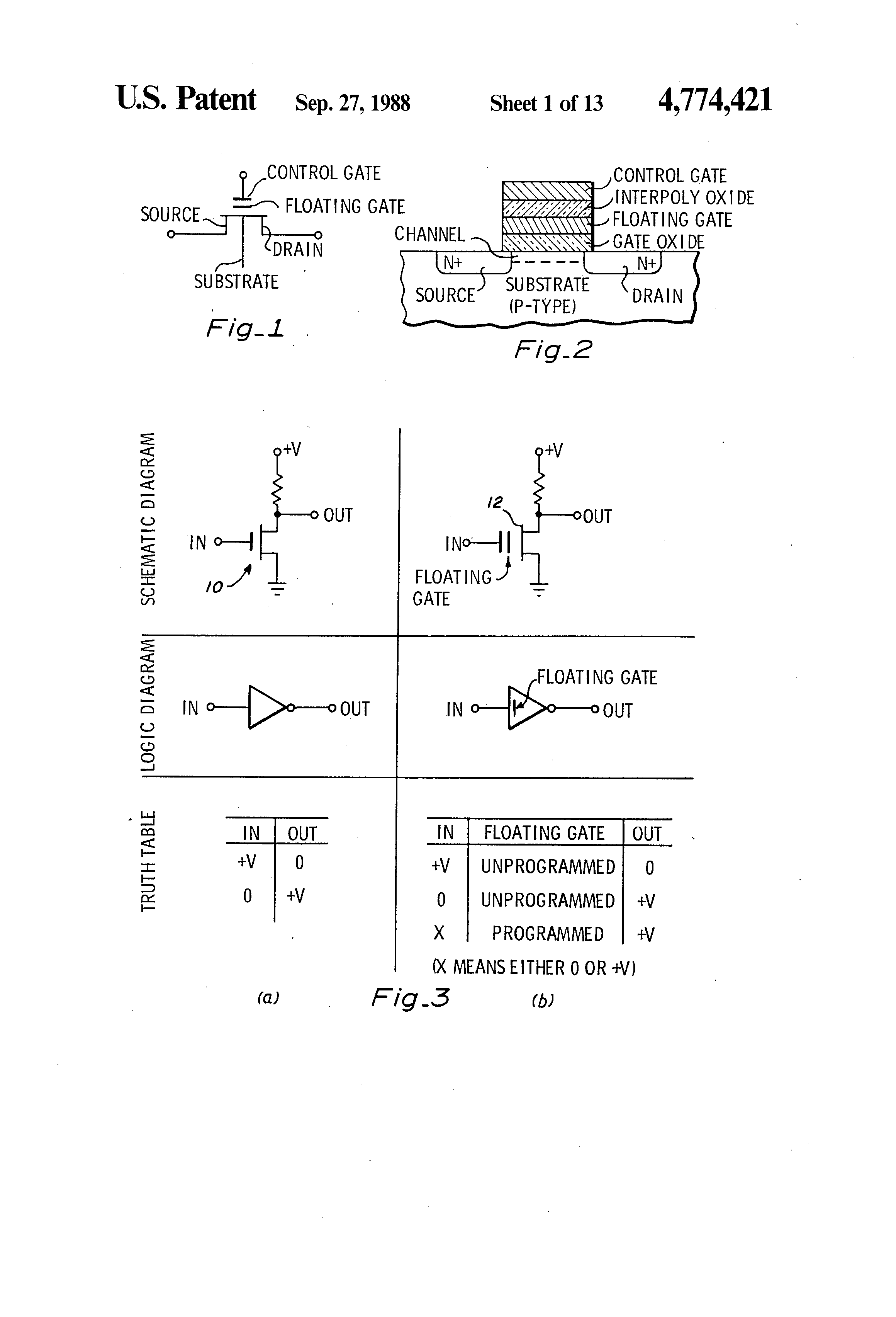
FIG. 1 is a diagram schematically representing a floating gate field effect transistor;

FIG. 2 is a diagram representationally showing in cross-section a two layer polysilicon field effect transistor;

FIG. 3 is a diagram pictorially comparing the schematic diagrams, logic symbols and truth tables of an MOS N-channel switching device and an MOS EPROM switching device;

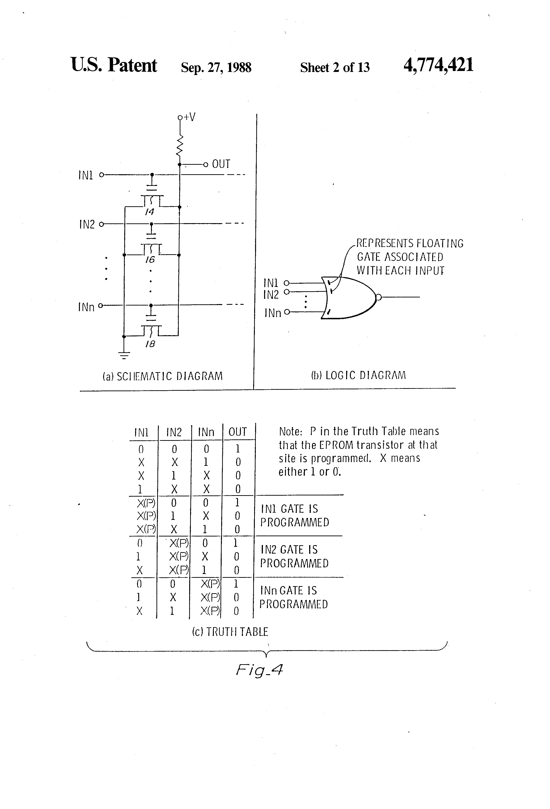
FIG. 4 is a diagram illustrating the circuit diagram, logic symbol and truth table of a NOR Gate device made using EPROM switching elements;

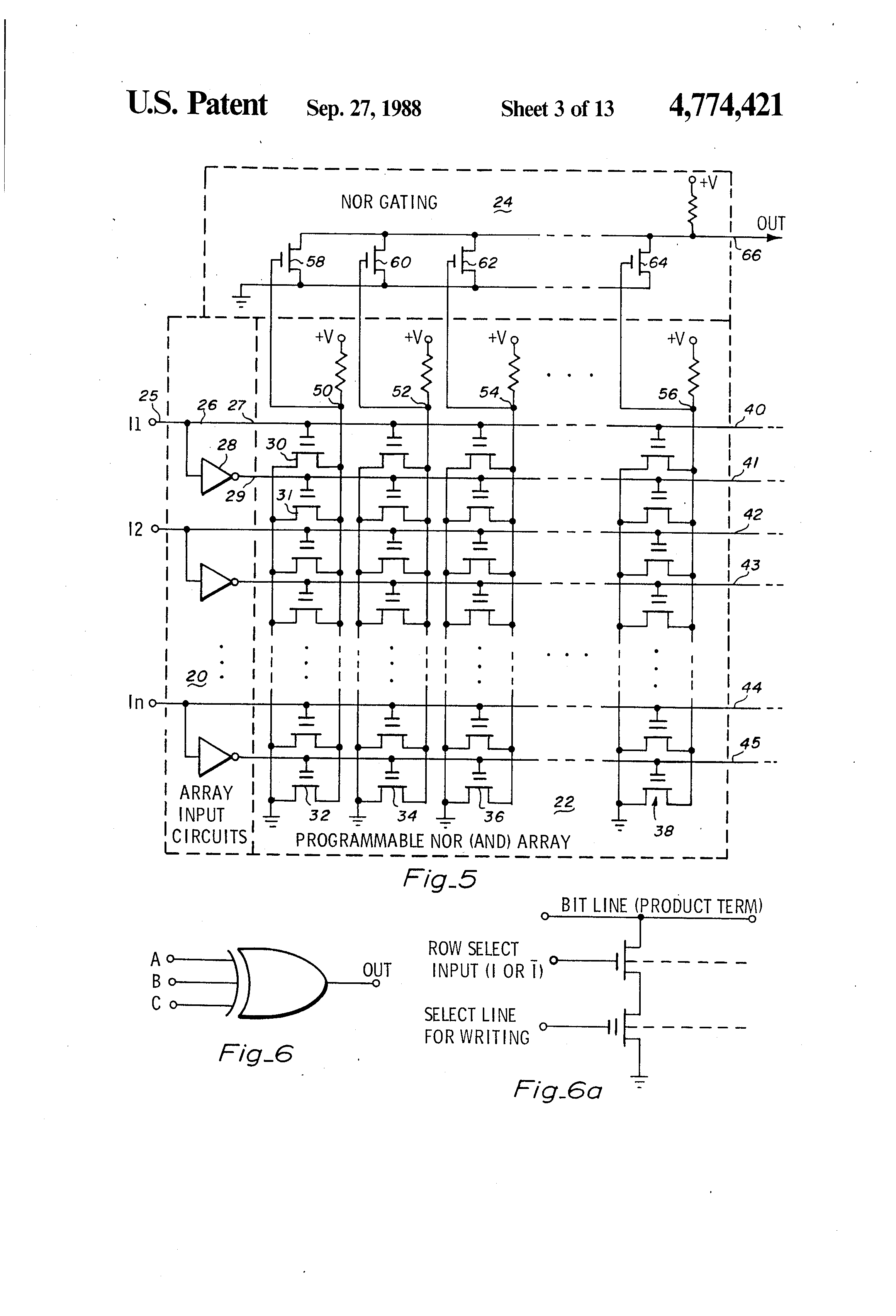
FIG. 5 is a schematic diagram showing an implementation of a sum-of-products generator using an array of EPROM NOR gates;

FIG. 6 is a logic symbol representation of an exclusive-or gate;

FIG. 6a is a schematic diagram illustrating an E2 PROM cell;

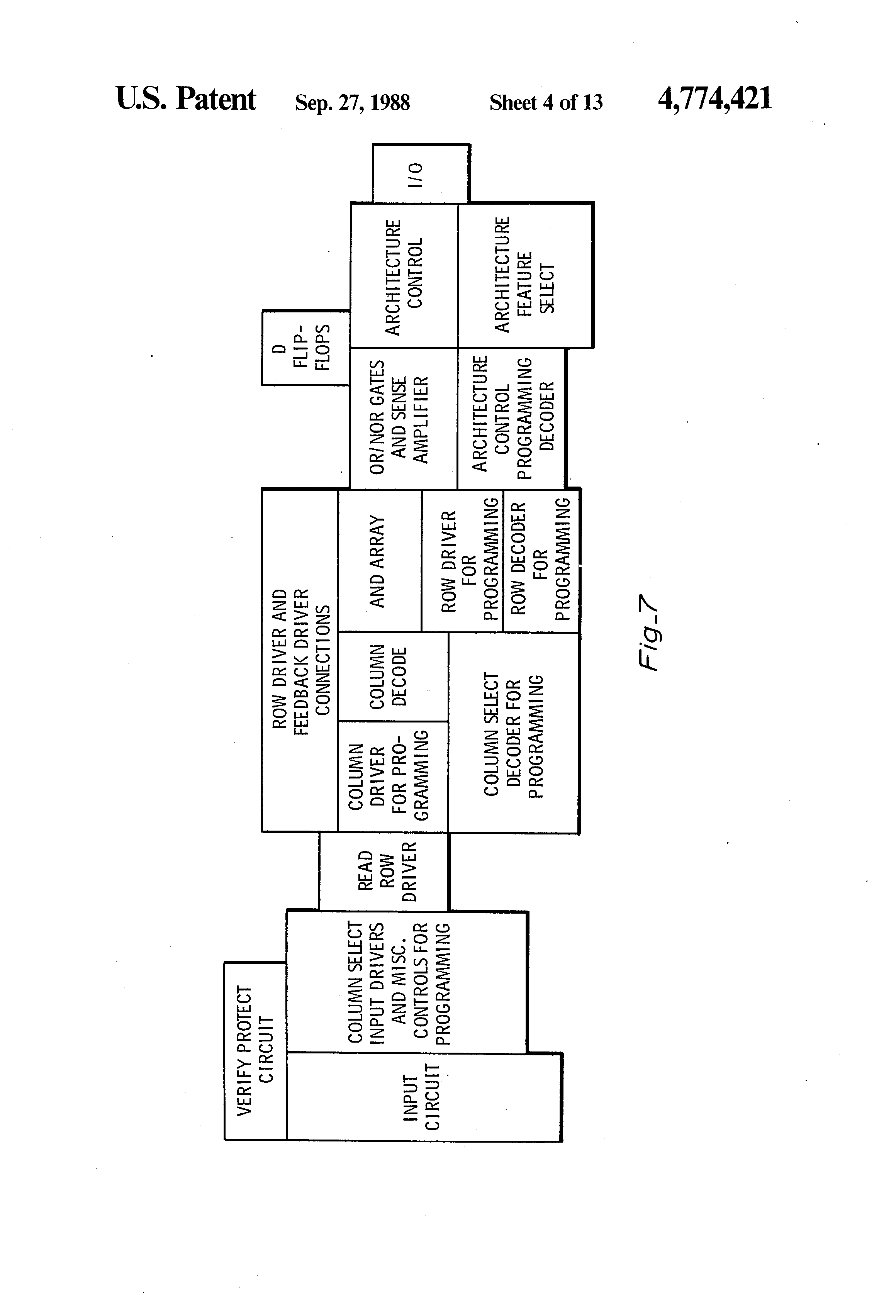
FIG. 7 is a diagram showing generally the major functional components of the EP300 electrically programmable logic array;

FIG. 8A is a block diagram showing the functional components utilized (for a typical data path) when the EP300 is operated in the Read Mode;

FIG. 8B is a generalized block diagram of the EP300 illustrating the major functional components and their interconnections when operated in the Read Mode;

FIG. 9 is a diagram schematically illustrating the Input Circuit of FIGS. 8A and 8B;

FIG. 10 is a diagram schematically illustrating the Read Row Driver of FIGS. 8A and 8B;

FIG. 11 is a diagram schematically illustrating the AND Array of FIGS. 8A and 8B;

FIG. 12 is a diagram schematically illustrating the OR/NOR Gates and Sense Amplifier of FIGS. 8A and 8B;

FIG. 13 is a diagram schematically illustrating the D Flip-Flop of FIGS. 8A and 8B;

FIG. 14 is a diagram schematically illustrating the Output Multiplexer portion of the Architecture Control Circuit of FIG. 8A and the OMUX circuit of FIG. 8B;

FIG. 15 is a diagram schematically illustrating the Feedback Multiplexer portion of the Architecture Control Circuit of FIG. 8A and the FMUX circuit of FIG. 8B;

FIG. 16 is a diagram schematically illustrating the I/O Driver of FIG. 8;

FIG. 17 is a block diagram showing the functional components utilized when the EP300 is operated in the Program Mode and Verify Mode;

FIG. 18 is a diagram schematically illustrating the HH Detect portion of the Input Circuit and Misc. Controls for the Programming circuit of FIG. 17;

FIG. 19 is a diagram schematically illustrating the Three State Detector Portion of the Input Circuit and Misc. Controls for Programming of FIG. 17 and its truth table;

FIG. 20 is a diagram schematically illustrating the ROW and Column NOR Decoder of FIG. 17;

FIG. 21 is a diagram schematically illustrating the Column Driver, Read Circuitry and Column Pass Transistors of FIG. 17;

FIG. 22A is a diagram schematically illustrating the Column Pass Gate Driver portion of the Column Select Decoder for Programming of FIG. 17;

FIG. 22B is a diagram schematically illustrating the Row Driver of FIG. 17;

FIG. 23 is a diagram schematically illustrating the Data I/O circuitry of FIG. 17;

FIG. 24 is a diagram schematically illustrating the Architecture Control Circuit of FIG. 17.

Technology Discussion

In order to understand the EP300, it is necessary to understand MOS floating gate technology. The diagrams shown in FIGS. 1 and 2 illustrate a 2 layer polysilicon transistor. An N-channel transistor is representationally shown but the basic mechanism applies to a P-channel transistor as well.

If it is assumed that the floating gate in the structure shown above is initially unprogrammed, then the transistor works as follows. Whenever a positive voltage greater than a certain threshold voltage (VT) is applied to the control gate, a channel is induced under the gate region which allows current to flow between the drain region and the source region. In a typical N channel floating gate device, VT is approximately 1.5 volts. The signals which are applied to the control gate are typically between 0 volts and 5 volts.

The effective threshold of the transistor can be changed by causing charges to be trapped on the floating gate. Electrons are caused to flow to the floating gate when high voltage (typically 21 volts) is applied to the control gate and the drain. When the high voltage is removed, charges remain trapped on the floating gate and cause the effective threshold to be increased to a value greater than the voltage which would be applied to the control gate during Normal Operation. The application of the high voltages and the subsequent charge trapping on the floating gate is called programming.

After the transistor shown above has been programmed, if a 5 volt signal is applied to the control gate, no channel will be created between the source and drain and no current will flow therebetween. This two layer transistor can be thought of as a programmable switch. In the unprogrammed state, the switch opens and closes in response to the application of 0 volts or 5 volts to the control gate. In the programmed state, the switch is always open regardless of whether 0 or 5 volts is applied to the control gate. Under normal environmental conditions, charges will stay trapped on the floating gate for very long periods of time (greater than 10 years). The typical application for this type of structure has heretofore been in the making of EPROMs (electrically programmable read-only-memories).

In the present invention, the EPROM transistor has been applied in a new way making the resultant structure suitable for implementing digital logic. The general structures will be described next.

Logic Structures Using EPROM Transistors

In the diagrams shown in FIG. 3, an inverter is shown in part (a) using a standard N-channel transistor 10 as the switching device and, in part (b) a floating gate transistor 12 is shown as the switching element. Below each schematic diagram, a logic gate representation and the corresponding truth table are shown. The truth table for the EPROM inverter in the unprogrammed state gives the same results as the normal N-channel inverter. However, when the floating gate is programmed, the output is always pulled high, independent of the input. Thus, logic functions can be programmed out of a circuit by programming the floating gate.

In part (a) of FIG. 4 a NOR gate using EPROM elements 14, 16, . . . 18 is illustrated. In this device, the output is only a function of the inputs corresponding to floating gates left unprogrammed. In part (b), the corresponding logic diagram is shown, and in part (c) the truth table for the circuit is set forth.

This circuit is a one dimensional array of EPROM elements which forms a NOR gate, the elements of which are selectively programmable. By extending this concept to a two dimensional array and then collecting the programmable NOR outputs in another set of NOR gates, electrically programmable logic arrays such as illustrated in FIG. 5 can be formed.

There are three major component parts of the circuit shown in FIG. 5: the Array Input circuits 20, the programmable NOR (AND) array 22, and the NOR Gating circuits 24.

The Array Input section consists of a set of subcircuits each including a conductive path 26 formed between an input node 25 and a first output node 27, and a second path including an inverter 28 coupled between node 25 and a second output node 29. Each input to circuit 20 and its complement thus become inputs to the Programmable NOR Array 22.

As illustrated in FIG. 5, the programmable NOR array 22 is comprised of a plurality of gates 30, 31 arranged in a two dimensional array of columns 32-38 and rows 40-45. The control gate electrodes of alternating rows 40, 42, . . . 44 of gates 30 are connected to an output node 27, while the corresponding gate electrodes of alternating rows 41, 43, . . . 45 of complement gates 31 are connected to an inverted output node 29 of the input circuit array 20. The drain regions of the transistors 30, 31 in each column of columns 32-38 are commonly coupled to a corresponding array output node of the nodes 50, 52, 54, . . . 56, and the source regions of the transistors of each column are coupled to circuit ground.

The outputs of the EPROM NOR gates feed into the gate electrodes of another NOR gate array 24 consisting of gates 58-64 which are connected in parallel and produce the desired output at an output node 66. This circuit can generate any logical function of the input variables by generating a so-called "sum-of-products" expression.

The example shown in FIG. 6 will be used to illustrate the case of a 3-input exclusive-or gate. The function of this circuit can be written in logic equation form as:

where ⊕ is the exclusive-OR operator. This expression can be expanded to the following sum of products

The groupings of variables on the right side of the equation are called "product terms" (e.g. A·B·C), and the product terms are "SUMed" together to produce the expression for OUT. By designating certain of the inputs (I1, I2, . . . ) of FIG. 5 as the variables A, B, C of FIG. 6 and by appropriately programming the array 22 of FIG. 5, the desired exclusive-or function of FIG. 6 can be realized. All logic equations can be expressed in this sum-of-products form. (See for example Logic Design Of Digital Systems by Dietmeyer).

The schematic diagram shown in FIG. 5 is an implementation of a sum-of-products generator in which the product generator is an array of EPROM NOR gates (columns) 32, 34, 36 and 38 whose outputs feed another NOR gate 24. In the illustrated example, the "PRODUCT" array 22 is programmable and the "SUM" array 24 is a fixed NOR gate. The fixed NOR gate 24 could alternatively be replaced by an EPROM NOR gate or an EPROM NOR array such that both the SUM array and the PRODUCT array are programmable. This would then be a realization of an EPROM Programmable Logic Array (EPLA) in accordance with the present invention.

Comparison to Other Competing Technologies

Although other programmable elements such as fuselink and EEPROM devices exist which are suitable for implementing Programmable Arrays, they each have certain disadvantages. In general, the fuse-link elements are less desirable than EPROM elements because:

(1) They take up more silicon area;

(2) They require high current to "blow" the fuse; and

(3) Once programmed, the fuse is physically blown and can not be repaired. These devices are therefor one time programmable.

The EEPROM element has two drawbacks:

(1) It requires more silicon area than does an EPROM; and

(2) The technology is less mature.

However it does have the advantage of being electrically eraseable and reprogrammable, thus allowing for logic functions to be changed in the system in which it is being used. This means that a logic system could modify itself based upon some set of conditions. This also means that real time alterable logic system or "adaptive logic systems" are possible. Furthermore, by replacing EPROM elements with EEPROM cells such as shown in FIG. 6a, an E2 logic array can be realized. In this diagram, N-channel transistors are assumed, but P-channel transistors could also be used with appropriate changes in signal voltages.

General Discussion of the EP300 Logic Diagram

FIG. 7 is an overall diagram showing the major functional components of the EP300 electrically programmable logic array.

The various circuit components will be described within the context of the several Modes of Operation of the EP300. These modes are: Read Mode (also referred to as normal operation), Program Mode, Verify mode, Preload Mode, Test Mode 1, and Test Mode 2.

Read Mode (Normal Operation)

As illustrated in the simplified block diagram of FIG. 8A, the Read Mode circuits consist of the Input Circuit 80, the Read Row Driver 82, the AND Array 84, the OR/NOR Gates and sense amplifier 86, the D Flip-Flop 88, the Architecture Control 90, and the I/O Driver 92.

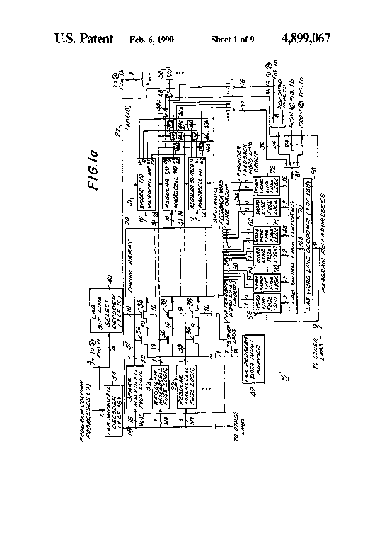
FIG. 8B is a further illustration of the EP300 showing the major functional blocks and their interconnection when operating in the Read Mode. As depicted, the device consists of a plurality of "macrocells" each including a programmable AND array, an OR/NOR array, a feedback row driver and an I/O driver and input circuit. Each input (designated as I) drives an Input Circuit (FIG. 9) which drives a Row Driver (FIG. 10) which drives all AND Arrays (FIG. 11). ((In the EP300, groups of Product Terms are ORed together by individual OR/NOR Sense Amp circuits (FIG. 12). We will, in this document, interchangably refer to each collection of Product Terms as an AND Array and also refer to all the Product Terms in the EP300 as the AND Array.)) As illustrated in FIG. 8B, all inputs go to all of the AND Arrays. The AND Array drives the OR/NOR Sense Amp (FIG. 12). The output of the OR/NOR Sense Amp is a Sum-of-Products of all signals which feed the AND Array. Each Sum term drives a D Flip-Flop (FIG. 13), a OMUX (FIG. 14) and an FMUX (FIG. 15). The output of the D flip-flop 2120 drives the OMUX and the FMUX. The OMUX drives the Output Driver (FIG. 16) which in turn drives the I/O pin. Each Output Driver is enabled by a Product Term from the AND Array. The FMUX can receive inputs from the OR/NOR Sense Amp or the D Flip-Flop of the Input Circuit connected to the Associated I/O pin. The FMUX drives a ROW driver circuit which in turn drives the AND Array.

Input Circuit--The input circuit 80 accepts a standard TTL level input signal, level shifts the signal and provides an output to the Read Row Driver 82. A simplified schematic of the input circuit 80 is shown in FIG. 9. As shown therein, an input signal comes in through a bonding pad 94 and passes through an input protection circuit consisting of resistors R1 and R2, and a so called "gate-aided-combine breakdown" N-channel transistor T1 which protects the gates of transistors T2 and T3 from static discharges. Transistors T2 and T3, and resistor R3 and capacitor C1 form a level shifter. TTL input levels are defined as VIL=0.8 volts and VIH=2.0 volts. T2 is a P-channel transistor and T3 is an N-channel transistor. The sizes of these transistors are chosen such that when the input is a VIL the voltage at Node 1 will be VCC (+5 volts) and when the input is VIH, Node 1 will be at less than the threshhold voltage of T5. When the input is at 2.0 volts (minimum VIH), both T2 and T3 are conducting. It is desireable to minimize the current flow from VCC thru T2 and T3 during this condition. R3 helps by causing a voltage drop between VCC and the source node of T2. This helps to turn T2 off because the source to gate voltage is reduced by the amount of the IR drop. The addition of resistor R3 increases the speed through the level shifter, reduces power dissipation and allows better sensing of TTL levels. Capacitor C1 is added to speed up the positive transition of Node 1 by helping to hold the source voltage of T2 constant when the input is switched from VIH to VIL. Transistors T4 and T5 form a normal CMOS inverter pair. However T5 is chosen to be larger than T4 to move the switching point lower. Thus as soon as Node 1 gets slightly higher than the turn on voltage VT of T5, Node 2 will go low. Inverter pair T6 and T7 act as a buffer for Node 2 and are capable of driving the Read Row Driver circuit shown in FIG. 10.

Read Row Driver-Referring to FIG. 10, the signal from the Input Circuit drives logic gates G11 and G12 of the Read Row Driver. G11 is a standard CMOS inverter and G12 is a standard CMOS two input NOR gate. Control signals NORMOP and NORMOPN disable the Read Row Driver circuit during Program Mode. The Read Row Driver circuit is active when NORMOP is a logic 1 and NORMOPN is a logic 0. Also VPC Well is at VCC. A logic 1 level from the Input Circuit 80 causes the outputs of G11 and G12 to go low turning T15 OFF and turning T14 ON pulling the output TO AND ARRAY to VCC and turning T13 off. A logic 0 from the Input Circuit 80 causes the output of G11 and G12 to go high turning T15 ON pulling the output toward VSS. At the same time, G11 pulls the gate of T14 high turning it OFF. As the output goes low, T13 is turned ON helping to turn T14 OFF. For each input, both "true" and "complement" signals must drive the AND array 84. Thus, there are two Read Row Drivers per Input. The second driver (not shown) has an extra inverter disposed between the Input Circuit and the Read Row Driver.

AND Matrix--The AND matrix is an array of EPROM NOR gates as discussed above. A single EPROM NOR gate is shown in FIG. 11 to illustrate the actual Pull-up circuit used.

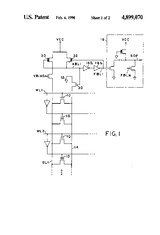
The gate of the N-channel pull-up circuit 96 is driven by the signal ENBLTOSA (Enable Bit Line To Sense Amp). This signal can be turned off during program mode to isolate the bit lines BL1, BL2, . . . BLn from VCC. Each bit line BLn is also connected through a column select transistor 98 to the column driver. These column select transistors are turned OFF during Normal Operation. The gates of the EPROM transistors 30 and 31 are driven by signals RRD and RRD which are representative of the true and complement signals from a Read Row Driver. In the EP300 there are 18 signal pairs; 10 from input signals and eight from feedback signals. Thus, each bit line BLn is a 36 input EPROM NOR gate. The bit line can also be thought of as a 36 input AND gate

The collection of bit lines will be referred to as the programmable AND matrix. In the EP300, bit lines are collected together in groups of 9. Eight of the nine bit lines go into the OR/NOR gating circuit 86 (FIG. 12) which will be discussed next, while the 9th bit line goes to control the tri-state of the associated output driver.

OR/NOR Gate, Sense Amplifier--As shown in FIG. 12, a grouping of eight bit lines are ORed together in the NOR Sense Amplifier. Transistors T1 through T13 are a sense amp-NOR gate. T1 through T8 receive their inputs from their respective bit lines. T9 acts as a pull-up. The "trip point" of the NOR gate is set by the threshold voltage of T1 through T8 plus the offset voltage created by current flowing through T12 and T13. This current flow is adjusted by T10 and T11. When the voltage of any of the bit lines exceeds the Variable Reference voltage, the output (OUT) will go low. Inverters G1 and G2 amplify the signal producing Sense Amp Output which goes to the D flip-flop 88 (FIG. 13) and the variable reference circuitry 87. The Sense Amp Output is fed back to the variable reference circuit through inverters G3 and G4. The feedback mechanism is such that if any bit line goes high, the Sense Amp Output will go low. After a slight delay caused by gates G3 and G4 and transistors T17 and T18, the output of G3 will also go low, causing the Variable Reference Signal to increase and in turn raise the trip point of the NOR gate Sense Amp. Thus, the trip point is adjusted according to the present state of the Product Term inputs. Adjusting the reference in this way allows the EP300 to sense a smaller signal swing and hence to operate faster.

D Flip-Flop--As illustrated in FIG. 13, the Sense Amp Output from FIG. 12 is input to a D Flip-Flop 88 after passing through the 2 input NAND gate 100, the other input of which is SET. The SET input comes from a single product term from the AND array 84. Whenever the SET line is a logic zero, the D input is forced to a logic 1 independent of the Sense Amp Output. The NAND gate 100 thus provides a synchronous SET to the D Flip-Flop where the SET is a function of any of the inputs to the AND array.

The Flip-Flop circuit is a conventional master-slave configuration using N and P channel pass transistors. As explained above, the Flip-Flop has a synchronous set and also has asynchronous reset. The RESET input is also a single term from the AND array. If both SET and RESET are asserted (low), the reset overrides set causing Q to go low and Q to go high. With neither SET nor RESET asserted, the Sense Amp Output is "captured" by the Flip-Flop 88 on the low to high transition of CLK. The Q and Q outputs are then passed to the Architecture Control circuit.

Architecture Control--The Architecture Control circuit consists of two pass-gate multiplexers which are designated the Output Multiplexer (OMUX) and the Feedback Multiplexer (FMUX). As depicted in FIG. 14, the OMUX has four data inputs. These are Q and Q from the Flip-Flop 88, and the Sense Amp Output signal and its complement which are designated COM and COM. (COM stands for combinatorial because it is a direct duplication of the combinatorial logic function produced by the AND array and the OR/NOR gate and Sense Amplifier circuit)

OMUX Circuit--The OMUX controls are QOUT, QBOUT, COMOUT and COMBOUT. The states of the OMUX control signals are determined by a set of EPROM bits which will be described below as part of the Architecture Feature Select Circuitry in FIG. 24. Because pass gates are used, only one OMUX control should ever be asserted (active high) or else a signal conflict at MI could exist. For example, if both QOUT and QBOUT are asserted, the Q and Q data inputs will be in conflict and the logic level at node MI will be indeterminate.

The OMUX allows the EP300 outputs to be configured as "registered" or "combinatorial" and be either active high or active low. The data which is passed to node MI is amplified by the inverter whose output (labeled ODI) becomes the input to the Output Driver. The ODI signal also feeds back to drive the gate of a P-channel transistor T19 whose source is tied to VCC and whose drain is tied to node MI. This transistor pulls node MI to a full VCC level. Without it, MI would be one VT voltage lower than the OMUX control signal (approximately 3.5 volts). This then helps to speed up the MI signal transition (to a logic one) and insure a good logic level at the inverter.

FMUX Circuit--The FMUX shown in FIG. 15 is of similar construction to the OMUX. It is a 3 input pass gate multiplexer. The data inputs are Q (from the Q output of the D Flip-Flop 88), COM (combinatorial data from the AND-OR arrays), and IOI (from the IO pad input). The corresponding controls are QFB, COMFB and IOFB. As with the OMUX, the states of these controls are determined by EPROM bits in the Architecture Feature Select block. There is an OMUX and an FMUX associated with each of the AND-OR blocks of the EP300.

I/O Driver--The signal ODI from the Output Multiplexer becomes the input to the Output Driver as shown in FIG. 16. ODN is the (active low) output disable signal which comes from a single product term from the AND Array (FIG. 11). The output circuit works as follows: The Output Driver is active whenever ODN is high. Both the N and the P channel transistors (N2, P2) between node 7 and node 8 are conducting as are the N and P channel transistors (N1, P1,) between ODI and node 6. Data from the OMUX (ODI) drives transistors N3 and P3 which in turn drive the output driver transistors N5 and P4. When ODI is a logic 1, the I/O Pad is driven to VCC through P4 and when ODI is a logic 0, the I/O pad is driven to VSS through N5. If signal ODN is driven low, transistors N1 and P1, and N2 and P2 are turned OFF. Node 8 is driven to VSS through N4, and node 6 is driven to VSS through N6. Node 7 is driven to VCC through P3. Under these conditions, both P4 and N5 are turned OFF. This is the tri-state condition for the output driver.

The I/O pins on the EP300 may be used as either inputs or outputs. When used as inputs, the Output Driver is disabled by means of the ODN signal described above. An input signal applied to the I/O pin goes to an Input Circuit as was shown in FIG. 9. The signal IOI in FIG. 16 is the amplified and level shifted version of the input signal applied to the I/O PAD and is passed to the FMUX.

PROGRAM MODE

Prior to using the EP300 in an application, it is necessary to program the EPROM Transistors in the AND array 84 and in the Architecture Feature Select block 90. FIG. 17 is a block diagram showing the functional components utilized when the EP300 is operated in the Program Mode and Verify Mode. Programming of an EPROM transistor is accomplished by applying high voltage to the gate and the drain. The high electric field from drain to source creates so-called "hot electrons". These hot electrons are attracted to the floating gate because of the high voltage. For 3 micron technology, a gate voltage of 21 volts and a drain voltage of approximately 16 volts will program the floating gate. Electrons with enough energy to jump from the drain to the floating gate remain trapped on the floating gate after the high voltages are removed. The presence of electrons on the floating gate cause the threshold voltage, as seen from the control gate, to be substantially increased such that under normal gate voltages (+5 V) it never will turn ON. Thus, an unprogrammed EPROM transistor will conduct with 5 volts on the gate and will not conduct with 0 volts on the gate, while a programmed EPROM transistor will not conduct in either state.

In order to program a single transistor in the AND array, a row and column selection must be made and appropriate high voltages applied. Some of the read circuitry described above must also be disabled so as to not cause damage. The circuits to be disabled are the Read Row Driver 82 (FIG. 10) and the pull-ups and the AND ARRAY 84 (FIG. 11). The Read Row Driver is disabled by causing NORMOP to go low. The AND ARRAY pull-ups are diabled by causing ENBLTOSA to go low. The Output Drivers must also be tri-stated because the I/O pins will be used as "program data" inputs. After a particular row and column are selected, the program data determines if the selected location is to be programmed or not.

Since all pins are used during normal operation, they must be redefined for programming. The program mode is entered whenever pin 11 is raised to a VHH level. VHH is a voltage greater than 10 volts and may be as high as 21 volts which is the VPP programming voltage. Several pins have VHH detection circuits which invoke various program, verify, and test modes. The following table lists the conditions required to enter various modes.

An EP300 is programmed in a manner similar to an EPROM memory. Taking Pin 11 to a VHH level causes the function of the pins to be redefined such that pins 2 through 9 become addresses which select a matrix row and column, and pins 12 through 19 become data inputs. The states of the data input lines determine whether a location will be programmed or left in its erased state. Eight bits can be programmed at a time.

Eight pins (2 thru 9) are defined as address input pins. If each has only two values (VIL, VIH) then only 256 locations can be selected. Actually, 324 array locations, 7 architectural locations and 1 security bit location must be accessible. In order to extend the address capability of the eight input lines, two pins (4 and 9) have three allowed values (VIL, VIH, VHH). This permits the addressing of all locations.

HH Detect Circuitry

The HH Detect Circuit is shown in FIG. 18. The allowable input values are VIL (VSS≦VIL≦0.8), VIH (2.0≦VIH≦VCC), and VHH (10≦VHH≦VPP). For any input value between VSS and VCC+VTP, the P-channel transistor P1 is not conducting. Since the N-channel transistor is always conducting, the voltage at HHDET is pulled to VSS through N1. (Inverters HHN and HH are simply buffers for node HHDET.) Thus, the signal at HH is zero whenever the input signal is a normal logic level (VIL or VIH).

If the input signal is raised above VCC+VTP, transitor P1 begins to conduct. Current flows from the input pad through P1 and N1 to VSS causing a voltage drop across N1. The transistor sizes are adjusted such that when the input signal is greater than 10 volts, the node HHDET is above the switching threshold of the inverter HHN. Thus, with an input level greater than 10 volts, the output from the second inverter HH is at a logic 1. The table below shows the situation.

As is illustrated in FIG. 19, input signals (applied to pins which have HH detectors) are connected to a normal Input Buffer (FIG. 9) and an HH detector circuit (FIG. 18). Signals from the Input Buffer can be logically gated with signals from the HH detector to create a third state. The three states are shown in the diagram of FIG. 19.

Row and Column Decoding--Internal Signals from input buffers or HH detectors are passed on to either a row decoder or a column decoder. These decoders are NOR decoders consisting of N-channel pull-down transistors with P-channel pull-ups to VCC. Except for the Architectural Decoder, these P-channel pull-ups are gated by a signal called NORMOP. By doing this, the NOR decoders only dissipate power during programming. A typical NOR Decoder is shown in FIG. 20.

Column Driver--Outputs from the Column Decoder drive the Column Pass Gate Driver (FIG. 22A) which, in turn drives the gates of the Column Pass Transistors 98 shown in FIG. 11. Referring to FIG. 11, one can see that one side of the Column Pass Transistor is tied to a bit line while the other side is joined in common with other Column Pass Transistors. The common node 99 is driven by the Column Driver for programming. FIG. 21 shows a group of Column Pass Transistors (typically 9) being drive by one Column Driver.

The Column Driver works as follows. When the Programming Mode is invoked, VPPOE (FIG. 21) (which comes directly from Pin 11) is at a VPP level (21 volts). ENCLVRF is at a logic 0 and ENCLVRFN is at a logic 1. NOR1 then reacts only to DATA. Assume DATA is at a logic 1, then DN is zero. This turns OFF transistor N4 and turns ON transistor N3 which pulls node 9 low which in turn pulls node 5 high. This causes transistor P1 to turn OFF and P2 to turn ON. With node 9 low, transistor N1 is OFF thus blocking any current flow from VPPOE to the COLUMNS. Thus with DATA at logic 1, the selected EPROM bit (as selected by the Column Pass Transistors and the ROW DRIVER) will stay in the erased state. Next, assume DATA is at a logic 0. Then DN will be 1 causing N4 to turn ON, pulling node 5 low. This in turn causes P1 to turn ON pulling node 9 high which causes N1 to turn ON and provides a current path fromm VPPOE through the Column Pass Transistor to the selected EPROM bit. Thus, with DATA at logic 0, the selected EPROM bit will be programmed.

In the VERIFY MODE, which will be discussed later, ENCLVRF is at a logic 1 thus overriding DATA by forcing DN and Node 9 to be low which turns transistor N1 OFF. This effectively disables the Column Driver during the VERIFY MODE.

Row Driver--The Row Driver is a tri-stateable driver whose inputs are zero to 5 volt levels from the ROW DECODER and whose outputs are zero to VPP. The ROW DRIVER outputs drive the gate terminals of the EPROM transistors in the AND ARRAY. A schematic diagram of the ROW DRIVER is shown in FIG. 22B.

The Row Driver works as follows: Assume the signal NORMOP is a logic 1 and NORMOPN is logic 0, which is the situation in the READ MODE described above. The signal RDIN from the ROW DECODER is at logic 0 because the decoder pull-up is OFF (see FIG. 19) VPCROW is a local power line which can be switched between VCC and VPP. During the READ MODE, VPCROW is equal to VCC. The signal RDIN is passed through transistor N1 pulling the gates of N2 and P2 low causing node 10 to go high and turning OFF P1 and P3. The pass transistor N3 is turned OFF by NORMOPN, isolating node 10 from node 11. Transistor N4 is turned ON by NORMOP causing node 11 to go low and turning OFF transistor N5. Thus both P3 and N5 are OFF and the output line ROW is left free to be driven by the READ ROW DRIVER described above.

Next, assume NORMOP is at logic 0 and NORMOPN is at logic 1. This is the case during programming. The Row Decoder (FIG. 20) is activated and RDIN can be either logic 0 (decoded) or logic 1 (not decoded). Transistor N3 is turned ON and N4 is turned OFF, thus, connecting node 10 to node 11. VPCROW is switched to the VPP level. Now, if RDIN is low, node 10 is pulled high turning P3 OFF and turning N5 ON, thus pulling ROW to Vss. If RDIN is at logic 1, N2 is turned ON pulling node 10 low. This turns P1 ON, thus pulling node 9 to VPP. Pass transistor N1 blocks the VPP level from the ROW DECODER. With node 9 at VPP, P2 is turned OFF and N2 is turned ON, pulling nodes 10 and 11 low. This turns P3 ON and N5 OFF and drives ROW to VPP. Since ROW drives the gates of the EPROM transistors, programming can now take place.

Row and Column decoding and driving is done simultaneously. A particular EPROM transistor is determined by the intersection of a row and a column.

Data Input For Programming--An EPROM transistor is selected at the intersection of the decoded row address and the decoded column. Whether the selected EPROM transistor is actually programmed, or left in its erased state, is determined by the DATA supplied to the Column Driver as explained above. The DATA line is driven by circuitry as shown in FIG. 23. When the PROGRAM MODE is invoked, the output driver is tri-stated. The signal PADBUS is at logic 1 and PADBUSN is at logic 0 causing the pass transistors (P1 and N1 in FIG. 23) to turn ON. The logical sense of DATA is inverted from that presented at the I/O Pad. From the previous discussion, this means that if a logic 0 is presented at the I/O pad, the selected EPROM transistor will remain in the erased state, while a logic 1 presented at the I/O pad will cause the EPROM transistor to be programmed.

The purpose of transistor P2 in FIG. 23 is to insure that DATA will be forced to a logic 1 whenever the pass transistors driven by PADBUS and PADBUSN are turned OFF.

Architecture Feature Programming--The architecture of the EP300 is determined by which paths are selected in the Output and Feedback Multiplexers of FIGS. 14 and 15. These multiplexers are in turn controlled by the Architecture Control Circuits (there is one for each multiplexer control) shown in FIG. 24. The Architecture Control Circuit consists of an EPROM transistor 200 whose state is "read" by a Schimdt trigger circuit 202. The output of the Schmidt trigger feeds a control gate 204 and the output of the control gate drives the particular multiplexer. There are seven control signals (4 output multiplexer controls and 3 feedback multiplexer controls) per output macro cell, requiring 7 Architectural Control Circuits per macro cell. There are eight macrocells thus requiring 56 Architecture control Circuits in the EP300.

The EPROM bits for Architecture Control are programmed as follows. (Refer to FIG. 24). In the Program Mode, NORMOP is at logic 0 turning OFF transistor N2 thus isolating the EPROM bit from FMUX. EPROM transistor 200 is programmed by raising ARDTCNTL at the gate of N1 to VPP. Also, the gate of 200 (PADFEED) is raised to VPP by the Architectural Program Decoder (FIG. 20) and a VPP level shifting circuit similar to the Pass Gate Driver (FIG. 22A). At the same time, line 14H10 is raised to a VPP-VT level by a column driver circuit similar to that shown in FIG. 21.

Referring now again to FIG. 24, to verify that the EPROM bit has been programmed, PADFEED and ARDTCNTL are taken to Vcc levels. The Architecture Control Program Driver is then disabled and a sense amplifier is connected to 14H10. The sense amplifier senses the state of the EPROM bit and passes the information to the associated Output Driver.

During the READ Mode, the following conditions apply. ARDTCNTL is taken to Vss thus disconnecting node 7 from line 14H10. PADFEED and NORMOP are taken to Vcc. The state of the EPROM bit can then be determined as follows: first, assume that the EPROM transistor 200 has been programmed. Transistor P1 will then pull node 7 and node 8 to Vcc. This will cause transistors N1 and N2 to turn ON pulling node 12 to Vss. During READ, PRELDBAR is at a logic 1. Thus, with node 12 at logic 0, IOFB will be at logic 1 which selects the I/O Pad as the signal to be passed through FMUX to the Feedback Row Driver. If the EPROM transistor had been in its erased state, nodes 7 and 8 would have been pulled high. This would force IOFB to a logic 0. Thus, in The Architecture Feature Select, a programmed EPROM bit selects a feature and an unprogrammed bit de-selects a feature. Initially, in the erased state, all features are de-selected.

Referring now again to FIG. 17, which is a block diagram of the EP300 for either the Program or the Verify Mode, and also referring to the EP300 Mode Select Table for the conditions which select the Verify Mode, it will be seen that the Verify Mode provides a means of interrogating the AND matrix and the Architecture Feature Select Matrix to determine which EPROM transistors have been programmed. Verify Mode is invoked by taking a pin 1 to Vhh. All other inputs are then directed through the INPUT CIRCUITS and appropriate control circuits to the ROW DECODER, the COLUMN SELECT DECODER and the ARCHITECTURE CONTROL PROGRAM DECODER. Although not shown in detail, these decoders are of a type well known to those skilled in the art of EPROM technology. Depending upon the state of the inputs, either eight locations in the AND ARRAY or one of the ARCHITECTURE FEATURES associated with each ARCHITECTURE CONTROL block will be directed through the I/O DRIVERS.

Verify is essentially the reverse process from Programming. The location to be interrogated during Verify is determined by the Input Signal exactly as it would be during Programming. The COLUMN DRIVERS and the ARCHITECTURE CONTROL PROGRAM DRIVERS are disabled and corresponding SENSE AMPLIFIERS are enabled. The data which is read by the SENSE AMPLIFIERS is directed to the output pins through the I/O DRIVERS.
TESTMODES

There are 2 special modes on the EP300. The following Table shows the control voltages necessary to enter the modes. Pin 2 at the HH level signifies the special modes. Pin 1 must be at Vil for the modes to operate properly.

(1) Testmode 1:

Testmode 1 is a reliability test to ensure the integrity of the EPROM elements. During this MODE, all EPROM elements except the VERIFY PROTECT EPROM bit will be stressed. Charge gain/charge loss, and oxide integrity problems may be detected when the mode is exercised in relation to TESTMODE 2 and/or VERIFY mode.

In TESTMODE 1, the gates of all EPROM elements will correspond to the voltage supplied on the VPP/OE pin (pin 11). One can stress all the gates from approximately 4 to 21 volts depending on the reliability test requirements. The supplies to drains of the matrix (2664 bits) and those in the architecture control section (56 bits) are all turned OFF. The voltages on the output pads will be either 1 or 0 depending on the programmed states of the matrix EPROM cells and the voltage supplied on pin 11.

(2) Testmode 2:

TESTMODE 2 is used to detect the VTs of programmed bits in the matrix. In the TESTMODE 2 circuit implementation of the EP300, only the highest VT of the 8 bits in a macrocell group may be detected. VTs of OE, SET and RESET bits cannot be read out using TESTMODE 2.

During TESTMODE 2, all the column pass transistors are turned OFF and an individual row of the matrix is selected by the inputs through the row decoder. The row line voltage is the voltage on the VPP/OE pin (pin 11). One of the multiplexers is turned ON to allow the data from the matrix sense amp to be read out.

Assuming all EPROM bits on the row are programmed, and if the gate voltage on the row is less than the programmed VT on the row of 8 cells, the output on the pad will be a logic 1. When the voltage on pin 11 is raised above the highest VT on that row, the output will trip to a logic 0.

The VT of an individual bit can be read out if only one bit per row is programmed. However, to test the VTs of all bits, the programming, TESTMODE 1 stressing or other reliability testing must be repeated 8 times.

Charge gain tests can also be made by monitoring the VT increases after extended high temperature bakes and/or stresses on unprogrammed cells.

Note that the VERIFY mode can also be used to detect more dramatic VT changes (i.e. changes in VT that will cause a complete change in the output logic state in the VERIFY mode).

PRELOAD MODE

The Preload Mode is entered by raising Pin 9 to Vhh. This causes the output driver to be tri-stated and forces the feedback multiplexer to get data from the I/O pad (independent of Architecture Selection). Thus, the normal feedback path (from the D-Flip-Flop in this case) is disabled and Pad Feedback is enabled. The inputs to the AND array are now all directly controlled by Input and I/O pads. The Preload condition is latched on a high-to-low transistion of the Clock (Pin 1). This frees up Pin 9 to be an input to the AND array.

The inputs to the AND Array act essentially like the "present-state" of a state machine. The output from the AND-OR array is the "next-state". When the Clock makes its transistion from low-to-high, the "next-state" is captured by the D Flip-Flop. Simultaneously, the output is enabled allowing the "next-state" to propagate to the Output.

The Preload mode allows the testing of an EP300 configured as a synchronous state machine by allowing external inputs to completely determine the "present-state". This allows fast and complete testing of all state transitions.

Although the present invention has been described in terms of a preferred embodiment, it will be appreciated that other alterations and modifications may be apparent to those skilled in the art. It is therefore intended that the following claims be interpreted as covering all such alterations and modifications as fall within the true spirit and scope of the invention.

Claims (27)

  1. In a programmable logic device including a plurality of electronic logic circuit means each having data input, output, and input/output terminals, and having signal feedback paths to said data input terminals and being responsive to input data signals received at said data input and input/output terminals and operative to perform particular logic functions and to generate commensurate circuit means output signals, and programmable means for configuring the architecture of said logic device so that each said logic circuit means is operative to perform a particular logic function, an improved programmable means comprising: a plurality of architecture control circuits each including: a reprogrammable memory device having an output terminal and having a programming potential input terminal by which said memory device may be programmed to either a first state to generate a logic signal of a first level or programmed to a second state to generate a logic signal of a second level at said memory device output terminal; programming means responsive to input program data signals and to an address signal corresponding to said reprogrammable memory device and operative to program said memory device by applying a programming potential to said memory device programming potential input terminal; sense means coupled to said memory device output terminal for sensing the level of a logic signal generated by said programmed memory device and for developing a commensurate control signal; and multiplexer means responsive to said control signal and operative to couple said logic circuit means output terminal either to an input/output terminal or to a signal feedback path thereby causing said logic circuit means to have one of a predetermined set of logic circuit configurations.
  2. In a programmable logic device as recited in claim 1 wherein each said reprogrammable memory device is an EPROM transistor.
  3. In a programmable logic device as recited in claim 1 wherein each said reprogrammable memory device is an EEPROM transistor.
  4. In a programmable logic device as recited in claim 1 wherein said logic circuit means includes register means for temporarily storing said circuit means output signal and for developing a stored output signal and an inverted stored output signal, and inverting means for receiving said output signal and developing an inverted output signal, and wherein said multiplexer means includes a plurality of transistor switching means connected between a plurality of data receiving terminals and a multiplexer output terminal, said data receiving terminals being coupled to receive said circuit means output signal, said inverted output signal, said stored output signal and said inverted stored output signal, each said switching means being coupled to receive a control signal from one of said architecture control circuits whereby one of said switching means may be rendered conductive and the others of said switching means may be rendered nonconductive by appropriately programming the corresponding reprogrammable memory device.
  5. In a programmable logic device as recited in claim 4 wherein each said reprogrammable memory device is an EPROM transistor.
  6. In a programmable logic device as recited in claim 4 wherein said reprogrammable memory device is an EPROM transistor.
  7. In a programmable logic device as recited in claim 1 wherein said logic circuit means includes register means for temporarily storing said circuit means output signal and for developing a stored output signal, and wherein said multiplexer means includes a plurality of transistor switching means connected between a plurality of data signal receiving terminals and a multiplexer output terminal, said data signal receiving terminals being coupled to receive said circuit means output signal, said stored output signal and an input signal from said input/output terminal, each said switching means being coupled to receive a control signal from one of said architecture control circuits whereby one of said switching means may be rendered conductive and the others of said switching means may be rendered nonconductive by appropriately programming the corresponding reprogrammable memory device.
  8. In a programmable logic device as recited in claim 7 wherein said reprogrammable memory device is an EEPROM transistor.
  9. In a programmable logic device as recited in claim 7 wherein each said reprogrammable memory device is an EPROM transistor.
  10. In a programmable logic device as recited in claim 1 wherein said logic circuit means includes: register means for temporarily storing said logic circuit output signal and for developing a stored output signal and an inverted stored output signal, and inverting means for receiving said output signal and developing an inverted output signal, and wherein said multiplexer means includes an output multiplexer having a first plurality of transistor switching means connected between a first plurality of data receiving terminals and a first multiplexer output terminal, said first data receiving terminals being coupled to receive said circuit means output signal, said inverted output signal, said stored output signal and said inverted stored output signal, each said switching means of said first plurality being coupled to receive a control signal from one of said architecture control circuits whereby one of said first plurality of switching means may be rendered conductive and the others of said first plurality of switching means may be rendered nonconductive by appropriately programming the corresponding reprogrammable memory devices; and a feedback multiplexer having a second plurality of transistor switching means connected between a second plurality of data receiving terminals and a second multiplexer output terminal, said second data receiving terminals being coupled to receive said circuit means output signal, said stored output signal and an input signal from said input/output terminal, each said transistor switching means of said second plurality being coupled to receive a control signal from one of said architecture control circuits whereby one of said second plurality of switching means may be rendered conductive and the others of said second plurality of switching means may be rendered nonconductive by appropriately programming the corresponding reprogrammable memory devices.
  11. In a programmable logic device as recited in claim 10 wherein each said reprogrammable memory device is an EPROM transistor.
  12. In a programmable logic device as recited in claim 10 wherein each said reprogrammable memory device is an EEPROM transistor.
  13. In an integrated circuit device including electronic logic circuit means having data input, output, and input/output terminals, and signal feedback paths to said data input terminals, and being responsive to at least one architecture control signal and operative to perform a particular electronic function on at least one input data signal received at a data input terminal to generate at least one commensurate circuit means output signal at said circuit means output terminal, and having programmable means for providing said architecture control signal to configure the architecture of said logic device so that said circuit means will perform a particular electronic function, an improved programmable means comprising: at least one architecture control circuit including: a reprogrammable memory device having an output terminal and a programming potential input terminal and which may be programmed either to a first state to generate a logic signal of a first level or programmed to a second state to generate a logic signal of a second level at said memory device output terminal; programming means responsive to input program data signals and to a corresponding address signal and operative to program said memory device to one of said states by applying a programming potential to said memory device programming potential input terminal; and sense means for sensing the level of a logic signal generated at said programmed memory device output terminal and for developing therefrom said architecture control signal for configuring the architecture of said logic device so that said circuit means will perform a particular electronic function.
  14. In an integrated circuit device as recited in claim 13 wherein each said reprogrammable memory device is an EPROM transistor.
  15. In an integrated circuit device as recited in claim 13 wherein each said reprogrammable memory device is an EEPROM transistor.
  16. In an integrated circuit device as recited in claim 13 wherein said electronic logic circuit means includes multiplexer means responsive to said architecture control signals and operative to couple said circuit means output terminal either to an input/output terminal or to a signal feedback path.
  17. In an integrated circuit device as recited in claim 16 wherein each said reprogrammable memory device is an EPROM transistor.
  18. In an integrated circuit device as recited in claim 16 wherein each said reprogrammable memory device is an EEPROM transistor.
  19. In an integrated circuit device as recited in claim 16 wherein said programmable means includes a plurality of architecture control circuits and wherein said electronic logic circuit means further includes register means for temporarily storing said circuit means output terminal signal and for developing a stored output signal, and wherein said multiplexer means includes a plurality of transistor switching means connected between a plurality of data receiving terminals and a multiplexer output terminal, said data receiving terminals being coupled to receive said circuit means output terminal signal, said stored output signal and an input signal from said input/output terminal, each said transistor switching means being coupled to receive a control signal from one of said architecture control circuits whereby one of said switching means may be rendered conductive and the others of said switching means may be rendered nonconductive by appropriately programming the corresponding reprogrammable memory devices.
  20. In an integrated circuit device as recited in claim 19 wherein each said reprogrammable memory device is an EPROM transistor.
  21. In an integrated circuit device as recited in claim 19 wherein each of said reprogrammable memory device is an EEPROM transistor.
  22. In an integrated circuit device as recited in claim 16 wherein said reprogrammable means includes a plurality of architecture control circuits, and wherein said electronic logic circuit means further includes register means for temporarily storing said circuit means output signal and for developing a stored output signal and an inverted stored output signal, and inverting means for receiving said circuit means output signal and developing an inverted output signal, and wherein said multiplexer means includes an output multiplexer having a first plurality of transistor switching means connected between a first plurality of data receiving terminals and a first multiplexer output terminal, said first data receiving terminals being coupled to receive said circuit means output signal, said inverted output signal, said stored output signal and said inverted stored output signal, each of said first plurality of switching means being coupled to receive a control signal from one of said architecture control circuits whereby one of said first plurality of switching means may be rendered conductive and the others of said first plurality of switching means may be rendered non-conductive by appropriately programming the corresponding reprogrammable memory devices; and a feedback multiplexer having a second plurality of transistor switching means connected between a second plurality of data receiving terminals and a second multiplexer output terminal, said second data receiving terminals being coupled to receive said circuit means output signal, said stored output signal and an input signal from said input/output terminal, each said switching means of said second plurality being coupled to receive a control signal from one of said architecture control circuits whereby one of said second plurality of switching means may be rendered conductive and the others of said second plurality of switching means may be rendered non-conductive by appropriately programming the corresponding reprogrammable memory devices.
  23. In an integrated circuit device as recited in claim 23 wherein each said reprogrammable memory device is an EPROM transistor.
  24. In an integrated circuit device as recited in claim 22 wherein each said reprogrammable memory device is an EEPROM transistor.
  25. In an integrated circuit device as recited in claim 16 wherein said programmable means includes a plurality of architecture control circuits, and wherein said electronic logic circuit means further includes register means for temporarily storing said circuit means output signal and for developing a stored output signal, and wherein said multiplexer means includes output multiplexer having a plurality of transistor switching means connected between a plurality of data receiving terminals and a multiplexer output terminal, said data receiving terminals being coupled to receive said circuit means output signal, said stored output signal and an input signal from said input/output terminal, each said switching means being coupled to receive a control signal from one of said architecture control circuits whereby one of said switching means may be rendered conductive and the others of said switching means may be rendered non-conductive by appropriately programming the corresponding reprogrammable memory devices.
  26. In an integrated circuit device as recited in claim 25 wherein each said reprogrammable memory device is an EPROM transistor.
  27. In an integrated circuit device as recited in claim 25 wherein each said reprogrammable memory device is an EEPROM transistor.

Publications

Related applications (7)

  1. US06/907,075

    Priority application

  2. US90/002916A

    Claims priority

  3. US06/742,089

    Claims priority

  4. US06/907,075

    Claims priority

  5. US90/002916A

    Parent application

  6. US06/742,089

    Parent application

  7. US06/907,075

    Patent family

Record timeline

  1. Priority claimed from US90/002916A

  2. Priority claimed from US06/742,089

  3. Application filed by Altera Corp

  4. Priority to US06/907,075

  5. Assigned to ALTERA CORPORATION

  6. Application granted

  7. Publication of US4774421A

  8. Assigned to ALTERA CORPORATION, A DELAWARE CORPORATION

  9. Anticipated expiration

  10. Expired - LifetimeCurrent

Legal events

  1. AS

    Assignment

    Owner name: ALTERA CORPORATION

    Free format text: CHANGE OF NAME;ASSIGNOR:ALTERA SEMICONDUCTOR CORPORATION;REEL/FRAME:004730/0103

    Effective date: 19841017

  2. STCF

    Information on status: patent grant

    Free format text: PATENTED CASE

  3. FEPP

    Fee payment procedure

    Free format text: PAYOR NUMBER ASSIGNED (ORIGINAL EVENT CODE: ASPN); ENTITY STATUS OF PATENT OWNER: LARGE ENTITY

    Free format text: PAYER NUMBER DE-ASSIGNED (ORIGINAL EVENT CODE: RMPN); ENTITY STATUS OF PATENT OWNER: LARGE ENTITY

  4. REMI

    Maintenance fee reminder mailed

  5. FPAY

    Fee payment

    Year of fee payment: 4

  6. SULP

    Surcharge for late payment

  7. FEPP

    Fee payment procedure

    Free format text: PAT HLDR NO LONGER CLAIMS SMALL ENT STAT AS SMALL BUSINESS (ORIGINAL EVENT CODE: LSM2); ENTITY STATUS OF PATENT OWNER: LARGE ENTITY

  8. FPAY

    Fee payment

    Year of fee payment: 8

  9. AS

    Assignment

    Owner name: ALTERA CORPORATION, A DELAWARE CORPORATION, CALIFO

    Free format text: MERGER;ASSIGNOR:ALTERA CORPORATION, A CALIFORNIA CORPORATION;REEL/FRAME:009015/0336

    Effective date: 19970325

  10. FPAY

    Fee payment

    Year of fee payment: 12

Patent citations (8)

  1. US4177452A

    Electrically programmable logic array

    International Business Machines Corporation · December 4, 1979 · Examiner cited

  2. JPS5715533A

    Logical array circuit possible for write-in

    Nec Corp · January 26, 1982 · Examiner cited

  3. US4495427A

    Programmable logic gates and networks

    Rca Corporation · January 22, 1985 · Examiner cited

  4. EP0055348A2

    Reprogrammable array logic systems

    International Business Machines Corporation · July 7, 1982 · Examiner cited

  5. US4458163A

    Programmable architecture logic

    Texas Instruments Incorporated · July 3, 1984 · Examiner cited

  6. US4490812A

    User reprogrammable programmed logic array

    Mostek Corporation · December 25, 1984 · Examiner cited

  7. US4508977A

    Re-programmable PLA

    Burroughs Corporation · April 2, 1985 · Examiner cited

  8. US4546273A

    Dynamic re-programmable PLA

    Burroughs Corporation · October 8, 1985 · Examiner cited

Non-patent citations (2)

  1. "Programmable Array Logic-PAL20RA10", pub. by Monolithic Memories, copyright 1978, pp. 1-15.
  2. Programmable Array Logic PAL20RA10 , pub. by Monolithic Memories, copyright 1978, pp. 1 15.

Cited by (194)

  1. USRE34363E

    Configurable electrical circuit having configurable logic elements and configurable interconnects

    Xilinx, Inc. · August 31, 1993

  2. US4870302A

    Configurable electrical circuit having configurable logic elements and configurable interconnects

    Xilinx, Inc. · September 26, 1989 · Examiner cited

  3. US4896296A

    Programmable logic device configurable input/output cell

    Lattice Semiconductor Corporation · January 23, 1990 · Examiner cited

  4. US4992679A

    Programming logic device with multiple independent feedbacks per input/output terminal

    Ricoh Company, Ltd. · February 12, 1991 · Examiner cited

  5. US5349670A

    Integrated circuit programmable sequencing element apparatus

    Advanced Micro Devices, Inc. · September 20, 1994 · Examiner cited

  6. US5510730A

    Reconfigurable programmable interconnect architecture

    Actel Corporation · April 23, 1996

  7. US5479113A

    User-configurable logic circuits comprising antifuses and multiplexer-based logic modules

    Actel Corporation · December 26, 1995

  8. US5015885A

    Reconfigurable programmable interconnect architecture

    Actel Corporation · May 14, 1991 · Examiner cited

  9. US5003202A

    Coincidence extendable programmable logic device

    Kawasaki Steel Corporation · March 26, 1991 · Examiner cited

  10. US4935648A

    Optimized E2 pal cell for minimum read disturb

    Advance Micro Devices, Inc. · June 19, 1990 · Examiner cited

  11. US4937475A

    Laser programmable integrated circuit

    Massachusetts Institute Of Technology · June 26, 1990 · Examiner cited

  12. US4930098A

    Shift register programming for a programmable logic device

    Intel Corporation · May 29, 1990 · Examiner cited

  13. US5183773A

    Method of manufacturing semiconductor device including such input protection transistor

    Mitsubishi Denki Kabushiki Kaisha · February 2, 1993 · Examiner cited

  14. US5142345A

    Structure of input protection transistor in semiconductor device including memory transistor having double-layered gate and method of manufacturing semiconductor device including such input protection transistor

    Mitsubishi Denki Kabushiki Kaisha · August 25, 1992 · Examiner cited

  15. US4963769A

    Circuit for selective power-down of unused circuitry

    Cypress Semiconductor · October 16, 1990 · Examiner cited

  16. US4967107A

    Programmable logic expander

    Plus Logic, Inc. · October 30, 1990 · Examiner cited

  17. US5781033A

    Logic module with configurable combinational and sequential blocks

    Actel Corporation · July 14, 1998 · Examiner cited

  18. US5091661A

    Methods and apparatus for reducing coupling noise in programmable logic devices

    Altera Corporation · February 25, 1992 · Examiner cited

  19. US5726586A

    Programmable application specific integrated circuit and logic cell therefor

    Quicklogic Corporation · March 10, 1998 · Examiner cited

  20. US5587669A

    Programmable application specific integrated circuit and logic cell therefor

    Quicklogic Corporation · December 24, 1996 · Examiner cited

  21. US6078191A

    Programmable application specific integrated circuit and logic cell

    Quicklogic Corporation · June 20, 2000 · Examiner cited

  22. US5594364A

    Programmable application specific integrated circuit and logic cell therefor

    Quicklogic Corporation · January 14, 1997 · Examiner cited

  23. US5986468A

    Programmable application specific integrated circuit and logic cell therefor

    Quicklogic Corporation · November 16, 1999 · Examiner cited

  24. US5168178A

    High speed NOR'ing inverting, MUX'ing and latching circuit with temperature compensated output noise control

    Intel Corporation · December 1, 1992 · Examiner cited

  25. US5485103A

    Programmable logic array with local and global conductors

    Altera Corporation · January 16, 1996 · Examiner cited

  26. US6759870B2

    Programmable logic array integrated circuits

    Altera Corporation · July 6, 2004

  27. US5619450A

    Drive circuit for flash memory with improved erasability

    Fujitsu Limited · April 8, 1997 · Examiner cited

  28. US5485102A

    Programmable logic devices with spare circuits for replacement of defects

    Altera Corporation · January 16, 1996 · Examiner cited

  29. US5262648A

    Medical diagnostic nuclear camera fork mounting with offset

    Independent Scintillation Imaging Systems (Isis) Inc. · November 16, 1993 · Examiner cited

  30. US5483178A

    Programmable logic device with logic block outputs coupled to adjacent logic block output multiplexers

    Altera Corporation · January 9, 1996 · Examiner cited

  31. US6023751A

    Computer system and method for evaluating predicates and Boolean expressions

    Hewlett-Packard Company · February 8, 2000 · Examiner cited

  32. USRE38651E1

    Variable depth and width memory device

    Altera Corporation · November 9, 2004 · Examiner cited

  33. US5850365A

    Sense amplifier with individually optimized high and low power modes

    Altera Corporation · December 15, 1998 · Examiner cited

  34. US5525917A

    Sense amplifier with feedback and stabilization

    Altera Corporation · June 11, 1996 · Examiner cited

  35. US5598109A

    Programmable logic array device with grouped logic regions and three types of conductors

    Altera Corporation · January 28, 1997 · Examiner cited

  36. US5537057A

    Programmable logic array device with grouped logic regions and three types of conductors

    Altera Corporation · July 16, 1996 · Examiner cited

  37. US5561631A

    High-speed minimal logic self blank checking method for programmable logic device

    Xilinx, Inc. · October 1, 1996 · Examiner cited

  38. US6815981B2

    Programmable logic array integrated circuit devices

    Altera Corporation · November 9, 2004

  39. US5543730A

    Techniques for programming programmable logic array devices

    Altera Corporation · August 6, 1996 · Examiner cited

  40. US5963049A

    Programmable logic array integrated circuit architectures

    Altera Corporation · October 5, 1999 · Examiner cited

  41. US5909126A

    Programmable logic array integrated circuit devices with interleaved logic array blocks

    Altera Corporation · June 1, 1999 · Examiner cited

  42. US6191608B1

    Techniques for programming programmable logic array devices

    Altera Corporation · February 20, 2001

  43. US5900743A

    Programmable logic array devices with interconnect lines of various lengths

    Altera Corporation · May 4, 1999 · Examiner cited

  44. US6259272B1

    Programmable logic array integrated circuit architectures

    Altera Corporation · July 10, 2001

  45. US6278291B1

    Programmable logic array devices with interconnect lines of various lengths

    Altera Corporation · August 21, 2001

  46. US5680061A

    Techniques for programming programmable logic array devices

    Altera Corporation · October 21, 1997 · Examiner cited

  47. US5689195A

    Programmable logic array integrated circuit devices

    Altera Corporation · November 18, 1997 · Examiner cited

  48. US6184705B1

    Techniques for programming programmable logic array devices

    Altera Corporation · February 6, 2001

  49. US6154055A

    Programmable logic array integrated circuit devices

    Altera Corporation · November 28, 2000 · Examiner cited

  50. US6204688B1

    Programmable logic array integrated circuit devices with interleaved logic array blocks

    Altera Corporation · March 20, 2001

  51. US5705939A

    Programmable logic array integrated circuits with segmented, selectively connectable, long interconnection conductors

    Altera Corporation · January 6, 1998 · Examiner cited

  52. US5986470A

    Programmable logic array integrated circuit devices

    Altera Corporation · November 16, 1999 · Examiner cited

  53. US5717901A

    Variable depth and width memory device

    Altera Corporation · February 10, 1998 · Examiner cited

  54. US6366121B2

    Programmable logic array integrated circuit architectures

    Altera Corporation · April 2, 2002

  55. US5592106A

    Programmable logic array integrated circuits with interconnection conductors of overlapping extent

    Altera Corporation · January 7, 1997 · Examiner cited

  56. US5850151A

    Programmable logic array intergrated circuit devices

    Altera Corporation · December 15, 1998 · Examiner cited

  57. US6392438B1

    Programmable logic array integrated circuit devices

    Altera Corporation · May 21, 2002

  58. US5614840A

    Programmable logic array integrated circuits with segmented, selectively connectable, long interconnection conductors

    Altera Corporation · March 25, 1997 · Examiner cited

  59. US6127846A

    Programmable logic array devices with interconnect lines of various lengths

    Altera Corporation · October 3, 2000 · Examiner cited

  60. US5796267A

    Tri-Statable input/output circuitry for programmable logic

    Altera Corporation · August 18, 1998 · Examiner cited

  61. US6396304B2

    Programmable logic array integrated circuits with blocks of logic regions grouped into super-blocks

    Altera Corporation · May 28, 2002

  62. US5541530A

    Programmable logic array integrated circuits with blocks of logic regions grouped into super-blocks

    Altera Corporation · July 30, 1996 · Examiner cited

  63. US5936425A

    Tri-statable input/output circuitry for programmable logic

    Altera Corporation · August 10, 1999 · Examiner cited

  64. US5543732A

    Programmable logic array devices with interconnect lines of various lengths

    Altera Corporation · August 6, 1996 · Examiner cited

  65. US5850152A

    Programmable logic array integrated circuit devices

    Altera Corporation · December 15, 1998 · Examiner cited

  66. US5631578A

    Programmable array interconnect network

    International Business Machines Corporation · May 20, 1997 · Examiner cited

  67. US5748009A

    Programmable logic cell

    International Business Machines Corporation · May 5, 1998 · Examiner cited

  68. US5717346A

    Low skew multiplexer network and programmable array clock/reset application thereof

    International Business Machines Corporation · February 10, 1998 · Examiner cited

  69. US5703498A

    Programmable array clock/reset resource

    International Business Machines Corporation · December 30, 1997 · Examiner cited

  70. US5671432A

    Programmable array I/O-routing resource

    International Business Machines Corporation · September 23, 1997 · Examiner cited

  71. US5646546A

    Programmable logic cell having configurable gates and multiplexers

    International Business Machines Corporation · July 8, 1997 · Examiner cited

  72. US5659717A

    Methods for partitioning circuits in order to allocate elements among multiple circuit groups

    Altera Corporation · August 19, 1997 · Examiner cited

  73. US5565793A

    Programmable logic array integrated circuit devices with regions of enhanced interconnectivity

    Altera Corporation · October 15, 1996 · Examiner cited

  74. US5764080A

    Input/output interface circuitry for programmable logic array integrated circuit devices

    Altera Corporation · June 9, 1998 · Examiner cited

  75. US6049225A

    Input/output interface circuitry for programmable logic array integrated circuit devices

    Altera Corporation · April 11, 2000 · Examiner cited

  76. US5631576A

    Programmable logic array integrated circuit devices with flexible carry chains

    Altera Corporation · May 20, 1997 · Examiner cited

  77. US5604712A

    Fast word line decoder for memory devices

    Lsi Logic Corporation · February 18, 1997 · Examiner cited

  78. US5970255A

    System for coupling programmable logic device to external circuitry which selects a logic standard and uses buffers to modify output and input signals accordingly

    Altera Corporation · October 19, 1999 · Examiner cited

  79. USRE40011E1

    System for coupling programmable logic device to external circuitry which selects a logic standard and uses buffers to modify output and input signals accordingly

    Altera Corporation · January 22, 2008

  80. US5825197A

    Means and apparatus to minimize the effects of silicon processing defects in programmable logic devices

    Altera Corporation · October 20, 1998 · Examiner cited

  81. US5670895A

    Routing connections for programmable logic array integrated circuits

    Altera Corporation · September 23, 1997 · Examiner cited

  82. US5592102A

    Means and apparatus to minimize the effects of silicon processing defects in programmable logic devices

    Altera Corporation · January 7, 1997 · Examiner cited

  83. US5672985A

    Programmable logic array integrated circuits with carry and/or cascade rings

    Altera Corporation · September 30, 1997 · Examiner cited

  84. US5691653A

    Product term based programmable logic array devices with reduced control memory requirements

    Altera Corporation · November 25, 1997 · Examiner cited

  85. US5666310A

    High-speed sense amplifier having variable current level trip point

    Cypress Semiconductor · September 9, 1997 · Examiner cited

  86. US6045252A

    Methods for allocating circuit design portions among physical circuit portions

    Altera Corporation · April 4, 2000 · Examiner cited

  87. US5915017A

    Method and apparatus for securing programming data of programmable logic device

    Altera Corporation · June 22, 1999 · Examiner cited

  88. US5768372A

    Method and apparatus for securing programming data of a programmable logic device

    Altera Corporation · June 16, 1998 · Examiner cited

  89. US5694058A

    Programmable logic array integrated circuits with improved interconnection conductor utilization

    Altera Corporation · December 2, 1997 · Examiner cited

  90. US5872463A

    Routing in programmable logic devices using shared distributed programmable logic connectors

    Altera Corporation · February 16, 1999 · Examiner cited

  91. US5835998A

    Logic cell for programmable logic devices

    Altera Corporation · November 10, 1998 · Examiner cited

  92. US5939790A

    Integrated circuit pad structures

    Altera Corporation · August 17, 1999 · Examiner cited

  93. US6384630B2

    Techniques for programming programmable logic array devices

    Altera Corporation · May 7, 2002

  94. USRE40423E1

    Multiport RAM with programmable data port configuration

    Xilinx, Inc. · July 8, 2008

  95. US5781032A

    Programmable inverter circuit used in a programmable logic cell

    International Business Machines Corporation · July 14, 1998 · Examiner cited

  96. US5844854A

    Programmable logic device with two dimensional memory addressing

    Altera Corporation · December 1, 1998 · Examiner cited

  97. US5880597A

    Interleaved interconnect for programmable logic array devices

    Altera Corporation · March 9, 1999 · Examiner cited

  98. US5999016A

    Architectures for programmable logic devices

    Altera Corporation · December 7, 1999 · Examiner cited

  99. US20030201794A1

    Programmable logic device with hierarchical interconnection resources

    Altera Corporation · October 30, 2003 · Examiner cited

  100. US6577160B2

    Programmable logic device with hierarchical interconnection resources

    Altera Corporation · June 10, 2003

  101. US5977793A

    Programmable logic device with hierarchical interconnection resources

    Altera Corporation · November 2, 1999 · Examiner cited

  102. US6798242B2

    Programmable logic device with hierarchical interconnection resources

    Altera Corporation · September 28, 2004

  103. US6300794B1

    Programmable logic device with hierarchical interconnection resources

    Altera Corporation · October 9, 2001

  104. US6417694B1

    Programmable logic device with hierarchical interconnection resources

    Altera Corporation · July 9, 2002

  105. US5898776A

    Security antifuse that prevents readout of some but not other information from a programmed field programmable gate array

    Quicklogic Corporation · April 27, 1999 · Examiner cited

  106. US6362649B1

    Field programmable gate array with mask programmed input and output buffers

    Actel Corporation · March 26, 2002

  107. US5959466A

    Field programmable gate array with mask programmed input and output buffers

    Actel Corporation · September 28, 1999 · Examiner cited

  108. US5936426A

    Logic function module for field programmable array

    Actel Corporation · August 10, 1999 · Examiner cited

  109. US6091258A

    Redundancy circuitry for logic circuits

    Altera Corporation · July 18, 2000 · Examiner cited

  110. US6166559A

    Redundancy circuitry for logic circuits

    Altera Corporation · December 26, 2000 · Examiner cited

  111. US6034536A

    Redundancy circuitry for logic circuits

    Altera Corporation · March 7, 2000 · Examiner cited

  112. US6646467B1

    PCI-compatible programmable logic devices

    Altera Corporation · November 11, 2003

  113. US5999015A

    Logic region resources for programmable logic devices

    Altera Corporation · December 7, 1999 · Examiner cited

  114. US7148722B1

    PCI-compatible programmable logic devices

    Altera Corporation · December 12, 2006

  115. US5982195A

    Programmable logic device architectures

    Altera Corporation · November 9, 1999 · Examiner cited

  116. US6127844A

    PCI-compatible programmable logic devices

    Altera Corporation · October 3, 2000 · Examiner cited

  117. US6271681B1

    PCI-compatible programmable logic devices

    Altera Corporation · August 7, 2001

  118. US20050081177A1

    Enhanced field programmable gate array

    Actel Corporation · April 14, 2005 · Examiner cited

  119. US7382155B2

    Enhanced field programmable gate array

    Actel Corporation · June 3, 2008

  120. US6150837A

    Enhanced field programmable gate array

    Actel Corporation · November 21, 2000 · Examiner cited

  121. US6320411B1

    Programmable logic array devices with enhanced interconnectivity between adjacent logic regions

    Altera Corporation · November 20, 2001

  122. US6184710B1

    Programmable logic array devices with enhanced interconnectivity between adjacent logic regions

    Altera Corporation · February 6, 2001

  123. US6628552B1

    Self-configuring input buffer on flash memories

    Intel Corporation · September 30, 2003 · Examiner cited

  124. US5896338A

    Input/output power supply detection scheme for flash memory

    Intel Corporation · April 20, 1999 · Examiner cited

  125. US5933026A

    Self-configuring interface architecture on flash memories

    Intel Corporation · August 3, 1999 · Examiner cited

  126. US5982196A

    Programmable logic device producing a complementary bit line signal

    Waferscale Integration, Inc. · November 9, 1999 · Examiner cited

  127. US6107820A

    Redundancy circuitry for programmable logic devices with interleaved input circuits

    Altera Corporation · August 22, 2000 · Examiner cited

  128. US6337578B2

    Redundancy circuitry for programmable logic devices with interleaved input circuits

    Altera Corporation · January 8, 2002

  129. US6222382B1

    Redundancy circuitry for programmable logic devices with interleaved input circuits

    Altera Corporation · April 24, 2001

  130. US6239612B1

    Programmable I/O cells with multiple drivers

    Altera Corporation · May 29, 2001

  131. US6417692B2

    Programmable I/O cells with multiple drivers

    Altera Corporation · July 9, 2002

  132. US6130555A

    Driver circuitry for programmable logic devices

    Altera Corporation · October 10, 2000 · Examiner cited

  133. US6052327A

    Dual-port programmable logic device variable depth and width memory array

    Altera Corporation · April 18, 2000 · Examiner cited

  134. US6392954B2

    Dual port programmable logic device variable depth and width memory array

    Altera Corporation · May 21, 2002

  135. US6335634B1

    Circuitry and methods for internal interconnection of programmable logic devices

    Srinivas T. Reddy · January 1, 2002

  136. US6121790A

    Programmable logic device with enhanced multiplexing capabilities in interconnect resources

    Altera Corporation · September 19, 2000 · Examiner cited

  137. US6384625B1

    Programmable logic devices with enhanced multiplexing capabilities

    Altera Corporation · May 7, 2002

  138. US6107824A

    Circuitry and methods for internal interconnection of programmable logic devices

    Altera Corporation · August 22, 2000 · Examiner cited

  139. US6255846B1

    Programmable logic devices with enhanced multiplexing capabilities

    Altera Corporation · July 3, 2001

  140. US6225823B1

    Input/output circuitry for programmable logic devices

    Altera Corporation · May 1, 2001

  141. US6107825A

    Input/output circuitry for programmable logic devices

    Altera Corporation · August 22, 2000 · Examiner cited

  142. US6288970B1

    Programmable logic device memory array circuit having combinable single-port memory arrays

    Altera Corporation · September 11, 2001

  143. US6278288B1

    Programmable logic device with enhanced multiplexing capabilities in interconnect resources

    Altera Corporation · August 21, 2001

  144. US6191998B1

    Programmable logic device memory array circuit having combinable single-port memory arrays

    Altera Corporation · February 20, 2001

  145. US6167560A

    One-cold encoding method for low power operation in a complex programmable logic device

    Xilinx, Inc. · December 26, 2000 · Examiner cited

  146. US6084427A

    Programmable logic devices with enhanced multiplexing capabilities

    Altera Corporation · July 4, 2000 · Examiner cited

  147. US6344755B1

    Programmable logic device with redundant circuitry

    Altera Corporation · February 5, 2002

  148. US6201404B1

    Programmable logic device with redundant circuitry

    Altera Corporation · March 13, 2001

  149. US6879183B2

    Programmable logic device architectures with super-regions having logic regions and a memory region

    Altera Corporation · April 12, 2005

  150. US6507216B1

    Efficient arrangement of interconnection resources on programmable logic devices

    Altera Corporation · January 14, 2003

  151. US6670825B1

    Efficient arrangement of interconnection resources on programmable logic devices

    Altera Corporation · December 30, 2003

  152. US6480028B2

    Programmable logic device architectures with super-regions having logic regions and memory region

    Altera Corporation · November 12, 2002

  153. US6201411B1

    Programmable integrated circuit having metal plate capacitors that provide local switching energy

    Xilinx, Inc. · March 13, 2001 · Examiner cited

  154. US6144225A

    Programmable integrated circuit having metal plate capacitors that provide local switching energy

    Xilinx, Inc. · November 7, 2000 · Examiner cited

  155. US6407576B1

    Interconnection and input/output resources for programmable logic integrated circuit devices

    Altera Corporation · June 18, 2002

  156. US20040251930A1

    Interconnection and input/output resources for programmable logic integrated circuit devices

    Altera Corporation · December 16, 2004 · Examiner cited

  157. US6989689B2

    Interconnection and input/output resources for programmable logic integrated circuit devices

    Altera Corporation · January 24, 2006

  158. US7839167B2

    Interconnection and input/output resources for programmable logic integrated circuit devices

    Altera Corporation · November 23, 2010

  159. US20030210073A1

    Interconnection and input/output resources for programmable logic integrated circuit devices

    Tony Ngai · November 13, 2003 · Examiner cited

  160. US7492188B2

    Interconnection and input/output resources for programmable logic integrated circuit devices

    Altera Corporation · February 17, 2009

  161. US20070030029A1

    Interconnection and input/output resources for programmable logic integrated circuit devices

    Altera Corporation, A Corporation Of Delaware · February 8, 2007 · Examiner cited

  162. US6614261B2

    Interconnection and input/output resources for programable logic integrated circuit devices

    Altera Corp · September 2, 2003

  163. US7317332B2

    Interconnection and input/output resources for programmable logic integrated circuit devices

    Altera Corporation · January 8, 2008

  164. US6894533B2

    Interconnection and input/output resources for programmable logic integrated circuit devices

    Altera Corporation · May 17, 2005

  165. US20080074143A1

    Interconnection and input/output resources for programmable logic integrated circuit devices

    Tony Ngai · March 27, 2008 · Examiner cited

  166. US6559715B1

    Low pass filter

    Xilinx, Inc. · May 6, 2003

  167. US7484081B1

    Method and apparatus for protecting designs in SRAM-based programmable logic devices

    Altera Corporation · January 27, 2009

  168. US7480763B2

    Versatile RAM for a programmable logic device

    Altera Corporation · January 20, 2009

  169. US7111110B1

    Versatile RAM for programmable logic device

    Altera Corporation · September 19, 2006

  170. US8566616B1

    Method and apparatus for protecting designs in SRAM-based programmable logic devices and the like

    Altera Corporation · October 22, 2013

  171. US8612772B1

    Security core using soft key

    Altera Corporation · December 17, 2013

  172. US20060080632A1

    Integrated circuit layout having rectilinear structure of objects

    Mathstar, Inc. · April 13, 2006 · Examiner cited

  173. US20070247189A1

    Field programmable semiconductor object array integrated circuit

    Mathstar · October 25, 2007 · Examiner cited

  174. US20090078987A1

    Programmable element and manufacturing method of semiconductor device

    Kabushiki Kaisha Toshiba · March 26, 2009 · Examiner cited

  175. US7910970B2

    Programmable element and manufacturing method of semiconductor device

    Kabushiki Kaisha Toshiba · March 22, 2011 · Examiner cited

  176. US20100100219A1

    Fabrication system of semiconductor integrated circuit, fabrication device, fabrication method, integrated circuit and communication system

    Takahiro Ichinomiya · April 22, 2010 · Examiner cited

  177. US8271117B2

    Fabrication system of semiconductor integrated circuit, fabrication device, fabrication method, integrated circuit and communication system

    Panasonic Corporation · September 18, 2012

  178. US20090144595A1

    Built-in self-testing (bist) of field programmable object arrays

    Mathstar, Inc. · June 4, 2009 · Examiner cited

  179. US8661394B1

    Depth-optimal mapping of logic chains in reconfigurable fabrics

    Iowa State University Research Foundation, Inc. · February 25, 2014

  180. US8438522B1

    Logic element architecture for generic logic chains in programmable devices

    Iowa State University Research Foundation, Inc. · May 7, 2013

  181. US8154942B1

    Integrated circuits with fuse programming and sensing circuitry

    Altera Corporation · April 10, 2012

  182. US9111121B2

    Method and apparatus for securing a programmable device using a kill switch

    Altera Corporation · August 18, 2015

  183. US8627105B2

    Method and apparatus for securing programming data of a programmable device

    Altera Corporation · January 7, 2014

  184. US8719957B2

    Systems and methods for detecting and mitigating programmable logic device tampering

    Altera Corporation · May 6, 2014

  185. US8736299B1

    Setting security features of programmable logic devices

    Altera Corporation · May 27, 2014

  186. US8461863B2

    Method and apparatus for securing a programmable device using a kill switch

    Altera Corporation · June 11, 2013

  187. US9152822B2

    Method and apparatus for securing programming data of a programmable device

    Altera Corporation · October 6, 2015

  188. US9767321B1

    Setting security features of programmable logic devices

    Altera Corporation · September 19, 2017

  189. US9852315B2

    Systems and methods for detecting and mitigating programmable logic device tampering

    Altera Corporation · December 26, 2017

  190. US10592699B2

    Systems and methods for detecting and mitigating of programmable logic device tampering

    Altera Corporation · March 17, 2020

  191. US11436382B2

    Systems and methods for detecting and mitigating programmable logic device tampering

    Altera Corporation · September 6, 2022

  192. US9026873B2

    Method and apparatus for securing configuration scan chains of a programmable device

    Altera Coporation · May 5, 2015

  193. TWI661676B

    Programmable array logic

    新唐科技股份有限公司 · June 1, 2019 · Examiner cited

  194. US10666262B2

    Programmable array logic

    Nuvoton Technology Corporation · May 26, 2020

Related Patents