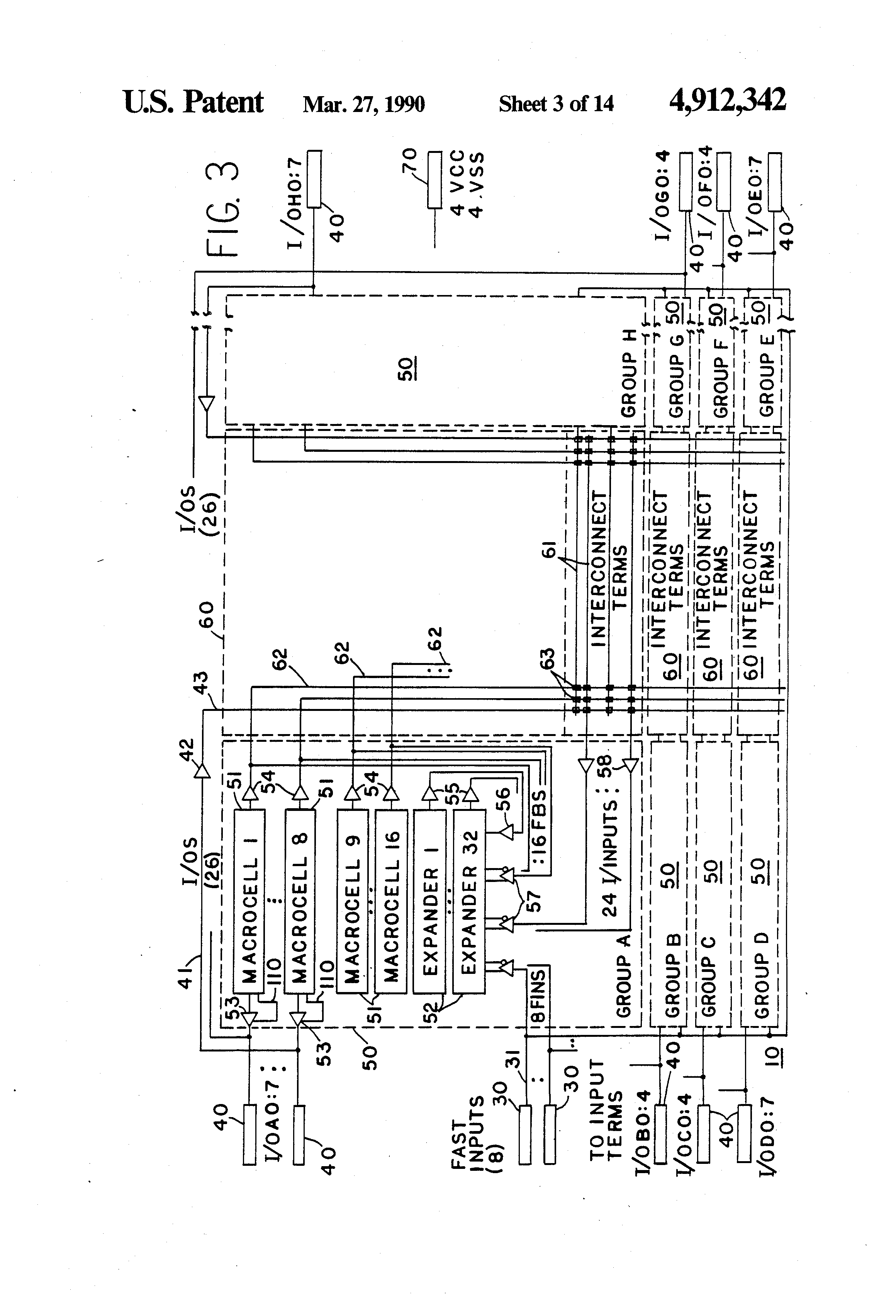
FIG. 3 is an overall block diagram of an illustrative embodiment of a programmable logic device 10 constructed in accordance with the present invention. The major elements shown in this diagram are "fast inputs" 30, I/O pads 40, logic array blocks (LABs) 50, and programmable interconnect array (PIA) blocks 60.
Input signals into chip 10 come from either fast inputs 30 or I/O inputs 40. Fast inputs 30 are routed via lines 31 to all of LABs 50. These signals drive into the array portion of the LAB through buffers 57 which provide both the true and complement polarity of the signal presented to the fast input pad. These lines are called fast inputs because they go directly to the LABs, in contrast to I/O inputs 40 which go indirectly to the LABs via PIA blocks 60. This can be seen by following representative signal line 41 from the pads labeled I/O0:7 (which represent eight such I/O pads) to buffer 42. After the signal has been suitably buffered by buffer 42, it drives into the PIA along line 43. By means of programmable elements 63 which are at the intersection of PIA word lines 43 and interconnect term lines 61, a signal which originated at one of the I/O pads 40 can be routed to any LAB 50 via the interconnect term 61 through buffer 58 and then into a true/complement LAB word line buffer 57. Signals propagating to an LAB via this path take additional time to traverse the PIA. Hence these signals are "slower" than the "fast" input lines 31 which go directly to the LAB as explained above. The reasons for providing these two different paths will be explained in due course.
A typical LAB 50 will now be explained in more detail. In this architecture there can be as many LABs as is deemed desirable. For example, in various preferred embodiments implemented to date we have used either four or eight LABs.
Each LAB 50 comprises macrocells 51 and expanders 52. Inputs to the LAB are provide by fast inputs via buffers 57, PIA inputs via interconnect terms 61 through buffers 58 and 57, feedback terms from macrocell outputs via buffers 54 and 57, and expander feedback terms via buffers 55 and 56. Two types of macrocells are provided. The only difference is the inclusion of output buffers 53 (plus their associated output enable (OE) signal 110 which provides the output tri-state control) in macrocells 1 through 8. Output buffers 53 selectively apply the associated macrocell outputs to I/O signal pins 40. Macrocells 9 through 16 have no associated output buffer and are therefore sometimes referred to as "buried" macrocells. In either case, the macrocells all have buffers 54 which take the signal generated by the macrocell and feed it to its own LAB (as described above) and also drive PIA word lines 62.
In the preferred embodiment shown in FIG. 3, each LAB 50 has 16 macrocells, 32 expanders, eight fast inputs, and 24 array inputs from the interconnect terms of the PIA. Each LAB also has a number of tri-stat output drivers 53: eight drivers 53 in the case of the LABs labelled group A, B, H, and G, and five drivers 53 in the case of the LABs labelled group C, D, F, and E. While we believe these choices to be optimum for the particular embodiment shown, other choices could be made without departing from the scope and spirit of the invention. For example, in another embodiment (shown in FIG. 7), there are four LABs, each of which has seven tri-state drivers In addition, the chip shown in FIG. 7 has eight dedicated inputs and four power/ground pins.
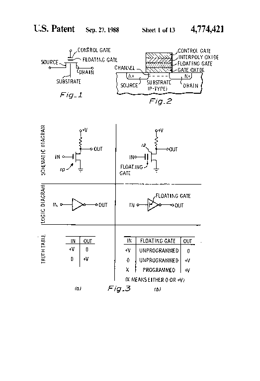
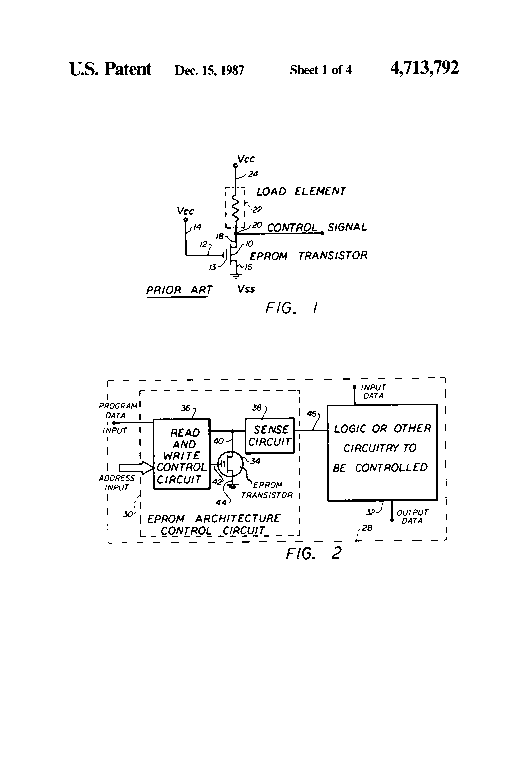
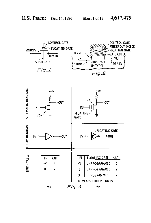
PIA blocks 60 will now be described with reference to FIG. 3. The PIA provides a mechanism for programmably routing signals from I/O input pins 40 to any LAB and from any LAB macrocell output to any other LAB. The PIA includes word lines 43 and 62 and bit lines 61. The bit lines are also labelled "interconnect terms" in FIG. 3. In the preferred embodiment shown, there are 52 word lines 43 which come from the I/O lines, and there are 128 word lines 62 which are driven from macrocell buffers 54. Interconnect terms 61 are perpendicular to the word lines. At the intersections of the word lines and bit lines are programmable elements 63 which, when programmed in one state, provide a connection between the associated word and bit lines, and which, when programmed in the other state, provide no such connection. In the preferred embodiment, the programmable elements are EPROM transistors. However, other types of programmable elements such as EEPROM transistors, fuses, anti-fuses, or other similar elements could be used without departing from the scope and spirit of the invention. There are 24 interconnect terms 61 feeding each LAB 50 in the embodiment shown. Again, this number is an estimate as to the optimum number for the device shown in FIG. 3, but a larger or smaller number could be used if desired. The entire PIA (i.e., all of PIA blocks 60 taken together) is therefore a programmable array with 180 word lines and 192 bit lines (eight groups of 24 bit lines).
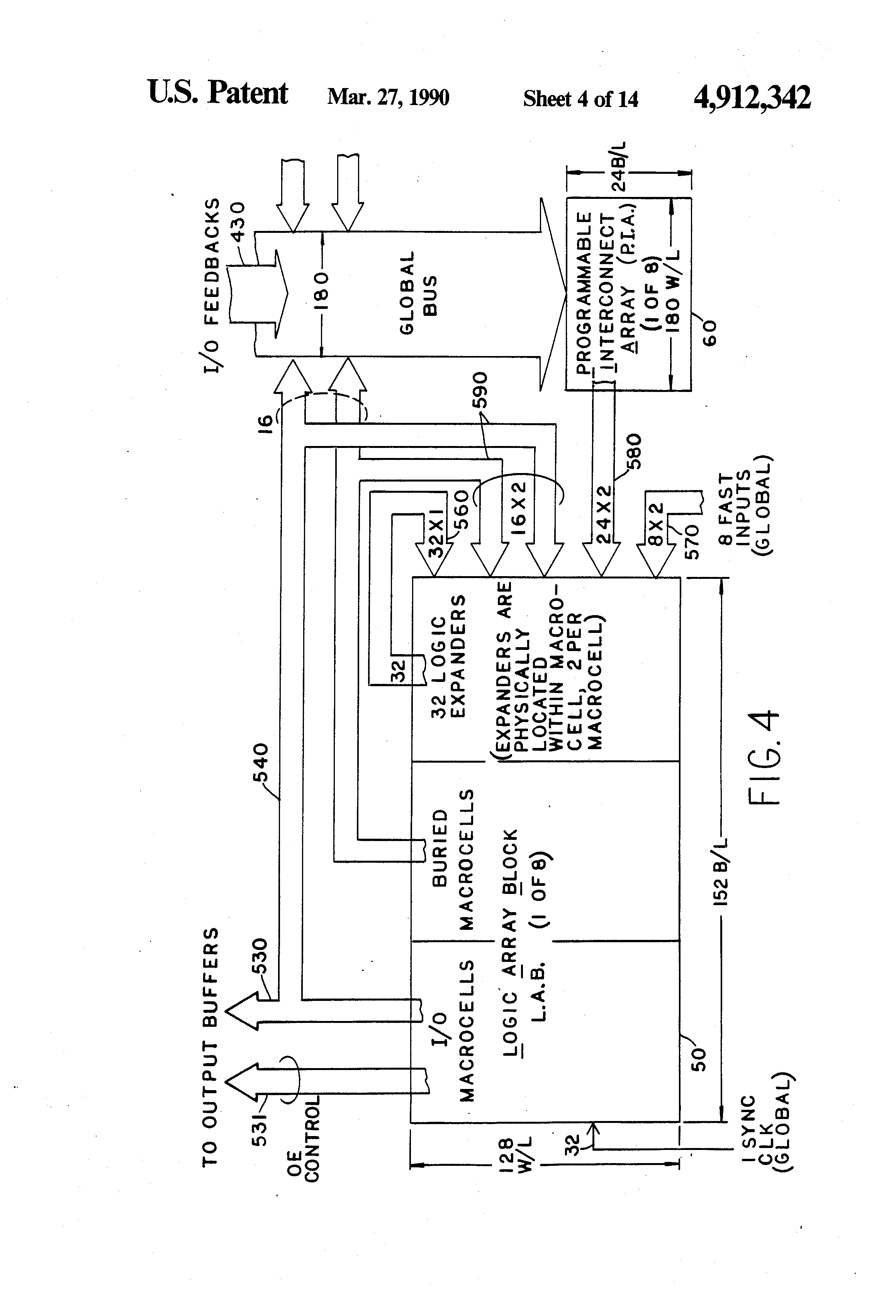
FIG. 4 is a block diagram showing a single LAB 50 and its associated PIA 60. This diagram shows, in concept, the signal routing to and from the LAB and the PIA. Lines going into the LAB are the fast inputs 570 shown as a group of 8×2=16 lines (true and complement signals), the interconnect terms 580 shown as a group of 24×2=48 lines (true and complement signals), the macrocell feedback lines 590 shown as two groups totaling 16×2=32 lines (true and complement signals), and the "expander" feedback lines 560 shown as a group of 32 lines (single polarity only). This totals to 128 word lines for each LAB in the embodiment shown. There ar 152 bit lines (P-terms) in each LAB. These will be described in detail in the discussion of FIG. 5. Shown in the diagram of FIG. 4 are the groups of signals 530 and 531 going to the output buffers labeled 53 in FIG. 3. Lines 530 provide the path for data from the macrocells to the output buffers, and lines 531 provide the path for the output enable (OE) signals from the OE P-terms. The PIA block 60 associated with this LAB is shown as having 180 word lines and 24 bit lines as previously described.
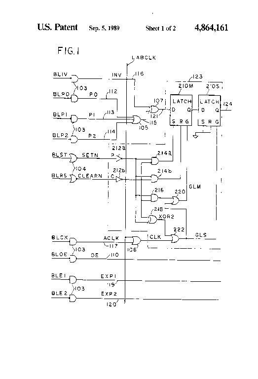
Referring now to FIG. 5, we can see more of the detail of one of the macrocells. In this case it is shown with an I/O buffer 53. If it were a buried macrocell, the only difference (at least pictorially) would be the absence of output buffer 53, the OE P-term structure (101, 103, 110), and I/O pin 40. The programmable array is shown a the intersection of word lines 102 nd bit lines 101. The label 51 refers to that part labelled "macrocell" in FIG. 3, and the label 52 refers to that part labelled "expander" in FIG. 3. Actually, in the physical layout of the chip, two expander P-terms are preferably grouped with the P-terms of each macrocell for convenience. In the description of FIG. 5, the word "macrocell" will be used to describe the entire collection of P-terms (including the two expander P-terms) and the associated logic gates 103-107, flip-flop 123, and output buffer 53, if present.
There are ten P-terms 101 in this macrocell. Each P-term receives inputs from the 128 word lines 102 (described earlier). There is a programmable element (similar to element 63 in the PIA) at the intersection of each bit line with each word line. A logical AND function of any of the word line variables can be formed by programming these elements. This is described in U.S. Pat. No. 4,617,479 and will not be repeated here. The correct logical outcome produced by each P-term is represented either as an active-low AND gate 103 or as a NOR gate 104. Those skilled in the art will recognize that other representations could be shown without departing from the scope and spirit of the invention. For example, an active-high AND gate could be used if one notes that the opposite polarity word line were used as its input and thus achieve the same logical result.
The purpose of each P-term is as follows: The P-term labelled OE is used as the output enable for the associated output buffer 53. If this were a buried macrocell, this bit line would be absent. SETN is used to control the preset of flip-flop 123. The next three terms, P0, P1, and P2, feed OR gate 105 which produces a logical sum-of-products at its output 115. This collection of P-terms, in conjunction with gate 105, forms the "programmable AND, fixed OR" function described in U.S. Pat. No. 4,124,899. The term labeled INV is used as an "invert control" for XOR gate 107. This allows for the creation of inverted sum-of-product functions at line 121. This will be recognized by those skilled in the art as expanding the number of possible functions which can be realized. In addition to acting as a static control for the inverted sum-of products option, the INV term can be used "dynamically" as a direct input to the XOR gate 107. For example, any logic function which can be reduced to (1) an EXCLUSIVE-OR of an AND function with an AND-OR function, (2 ) an EXCLUSIVE-OR of an OR function with an OR-AND function, (3) an EXCLUSIVE-OR of an OR function with an AND-OR function, or (4) an EXCLUSIVE-OR of an AND function with an OR-AND function can be implemented in detail in FIGS. 8a and 8c; the dollar sign in FIG. 8a represents the EXCLUSIVE-OR function.) ACLK is used to create an "asynchronous" clock signal for flip-flop 123 in conjunction with gate 106 and gates 109 and 108. CLEARN is used to control the "Clear" line on flip-flop 123. EXP1 and EXP2 are the "expander" P-terms. Note that each expander 52 preferably includes only a single P-term.
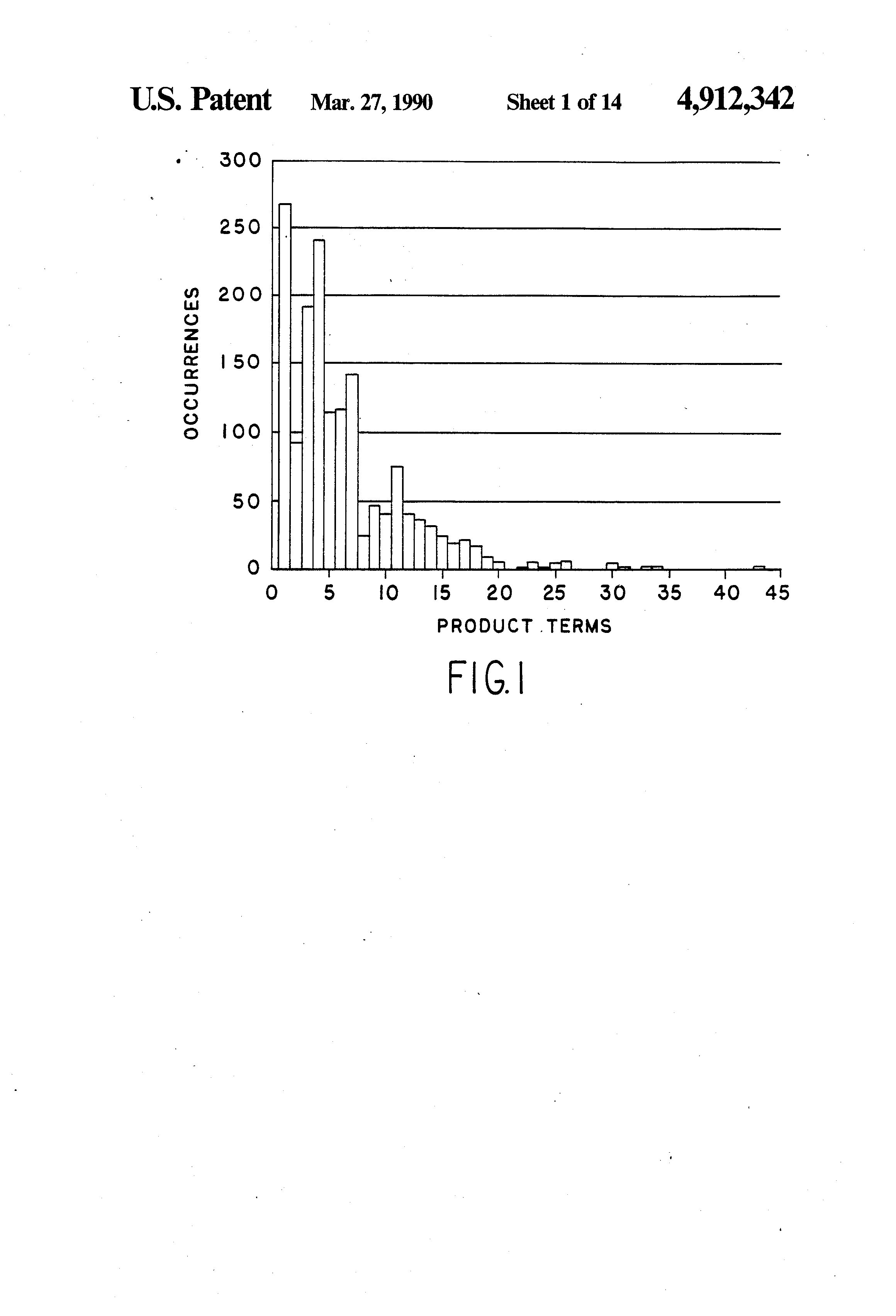
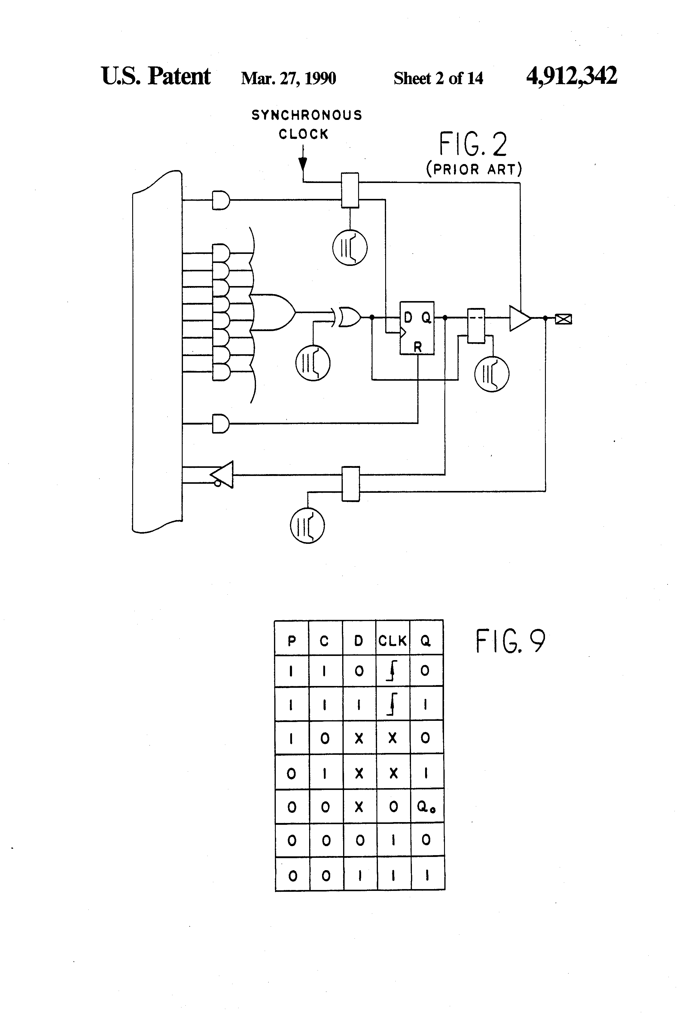
Our assignee has studied the most often used logic functions in relation to a variety of possible architectures. In particular, the AND-OR-XOR structure of P0, P1, P2, OR gate 105, and XOR gate 107 was analyzed assuming both less than three AND P-terms (e.g., two AND P-term) feeding OR gate 105, and more than three AND P-terms (up to eight P-terms such as is used in the prior art macrocell of FIG. 2) feeding the OR gate. The classes of functions included the following: adders, comparators, counters, decoders, demultiplexers, parity generators, and shift registers. The purpose of the study was to evaluate the architecture of the present invention relative to the prior art architecture of FIG. 2. The present new architecture is a combination of three programmable ANDs, a fixed OR, and an XOR, with single-P-term "expanders". This architecture is believed to be superior to both the prior art structure shown in FIG. 2 and to the single-P-term architectures proposed in the above-mentioned Goetting et al. reference. The study bore this out and reached several other important conclusions. It was found that having less than three P-terms feeding the OR gate is very restrictive when doing counters and shift registers. For all other functions examined, three P-terms feeding the OR gate was always as good as four P-terms feeding the OR. (This is only true assuming that in either case there is the additional BLIV P-term and XOR gate 107.) The prior art eight-P-term architecture is only superior for a very limited group of functions (for example, multiplexers with more than four inputs). The study also demonstrated that having approximately two expander P-terms per macrocell was more than sufficient to accommodate the less common functions which require many P-terms.
Expanders 52 play an important role in this new architecture. As their name implies, these P-terms allow for growth. That is, they allow for implementation of those (less common) functions which do not fit within the three-P-term limit (for example, an 8-to-1 multiplexer can be fit into 9 expanders). Expander P-terms anywhere in the LAB can be used to form elements of these more complex functions, and then the outputs of these P-terms are combined using another P-term (typically one of the P-terms feeding a fixed OR gate 105) (see, for example, FIG. 8f). Functions formed with expander P-terms can also be used to feed other expanders on single P-terms such as INV, ACLK, SETN, CLEARN, or OE. Also, there are often common P-terms which can be used by a number of logic functions. These common P-terms can be formed by he expanders and then fed to those functions (which are likely to be implemented in a programmable AND fixed OR section) for which they are required. FIG. 8e shows an example of a logic expression which requires more than three P-terms which can be factored into expressions which can be formed using the expander P-terms and recombined using another P-term (typically his will be a P-term which feeds the fixed OR gate). In FIG. 8e, the original expression has been factored such that two factors are implemented in two expanders and then combined with the remainder of the expression in one of the P-terms feeding the fixed OR gate. The original expression was:
This expression can be factored and rewritten as:
The common factors X*Y are formed on the P-term feeding the fixed OR gate, while the remaining factors (A+B+C) and (D+E) are formed on each of two expanders and fed to the P-term which contains the X*Y term. In this example, an expression which would have required six P-terms to implement can now be done in three P-terms. Suppose further that either the expression (A+B+C) or the expression (D+E) were required by some other macrocell or macrocells. These same expressions formed on the expander P-terms could be used again by those other macrocells. Thus an expression generated on the expanders can be amortized across all of the macrocells which have the expander's outputs as word line inputs. This again results in an overall saving of valuable P-term resources. Examples of various types of logic functions which can be fit into the P-term structure of the present invention are shown in FIGS. 8a through 8g. Latches require only two expanders. This structure is shown in FIG. 8h.
Continuing now with FIG. 5, XOR gate 107 receives its inputs from OR gate 105 and P-term INV. Those skilled in the art will recognize that if the logic signal on line 116 is 0, then the output of XOR gate 107 (line 121) will have the same logic value as input 115. On the other hand if line 116 is 1, then 121 Will be the logical inversion of 115. In addition to allowing for inverted sum-of-product functions, or positive or inverted product-of-sum functions, this structure, in conjunction with a D flip-flop such as 123, also allows for emulating other flip-flop types such as T, J-K and R-S. Emulation of various flip-flop types using array logic and XOR gates is the subject of U.S. Pat. No. 4,677,318. When using the expander P-terms as an AND array and the P-terms feeding the OR gate 105 as an OR array, the INV signal 116 needs to be set to a logic 1.
Flip-flop block 123 appears to be a simple D flip-flop with active low preset (P) and clear (C). However, this is done for simplicity of illustration of the macrocell. FIG. 9 is a truth table which explains the full functionality of element 123. Note that if P=C=1, then 123 is an edge-triggered flip-flop. At the rising edge of CLK (line 122 in FIG. 5), whatever data is present at the D input 121 is transferred to the Q output 124. If P is 0 and C is 1 then the Q output will be forced to 1 independent of the state of CLK or D. If C is 0 and P is 1, then the Q output will be forced to 0 independent of the state of CLK or D. To those skilled in the art, the case where P=C=0 is an illegal condition and is not defined. For flip-flop 123, however, when P=C=0, the flip-flop is redefined as shown in FIG. 9. It thus becomes a "flowthrough latch". Then, whenever line 122 is high, the Q output takes the value of whatever is on the D input. Whenever line 122 is low, the Q output holds the value that was present at the D input when line 122 went low. If line 122 is held high (for example, by programming P-term ACLK high), then signals will propagate directly from 121 to 124. This is the same "combinatorial" function as was provided by multiplexers and architectural control EPROM bits on prior art EPLD circuits. The present new design is simpler, faster, and provides greater functionality. As has been mentioned, a preferred structure for implementing flip-flop 123 is shown in concurrently filed, commonly assigned, co-pending Pat. application Ser. No. 190,530, which is hereby incorporated by reference herein.
The output signal 124 from flip-flop 123 (1) goes to the input of output driver 53, (2) feeds back (via buffer 54) to a word line driver 57 of its own LAB, and (3) drives one of the word lines of the PIA (indicated as line 62 in FIG. 3). This signal 124 can be used by any other LAB via its connection through the PIA. The signal also feeds a conventional tristate I/O buffer 53 such that if the buffer is enabled by line 110, the signal from 124 will drive off chip through I/O pin 40. I/O pin 40 can also provide an input path from off chip via line 41. This line drives buffer 42 (FIG. 3) whose output becomes one of the word lines for the PIA shown as line 43 in FIG. 3. I/O buffer 53 can be dynamically controlled by the OE P-term, in which case pin 40 may be both an input and an output depending upon the state of line 110. Alternatively, by programming the chip such that OE is always 0 buffer 53 will always be disabled, in which case I/O pin 40 can be used permanently as an input. Thus each of I/O pins 40 can be configured as input, output, or bi-directional input/output terminals. Because of the feedback of signal 124 to the LAB and the PIA, and the I/O input line 41, disabling of the output driver 53 does not result in the loss of the macrocell's functionality. This is a significant advantage over some prior art devices.
Turning now to the clock structure for the LAB, this structure includes inverter 109, AND gate 108, OR gate 106, and P-term ACLK. Three modes of operation are anticipated as follows:
COMBINATORIAL MODE: In this case, P=C=0 as previously described. Further, the ACLK P-term is programmed to always be 1, and line 122 is therefore also always 1. Whatever data is present at line 121 will pass through flip-flop 123 and appear at line 124.
ASYNCHRONOUS MODE: In this case, the line labeled ECKN (which is an extra P-term (not shown) in the LAB) is programmed to be 1. This means that line 125 is logic 0. Then line 122 is directly controlled by the state of the ACLK P-term. ACLK can be any (inputs active-low) AND function of any of the word line variables. Each flip-flop in the LAB has its own separate ("asynchronous") P-term clock.
SYNCHRONOUS MODE: P-term ACLK is programmed to be always 0. Also, ECKN is programmed to be 0 and thus ECK is 1. This allows the signal EXT.(SYNC.)CLK. on line 32 to propagate through AND gate 108 and appear on line 125. EXT.(SYNC.)CLK. line 32 comes from an input pad (one of the "fast inputs") not shown. This signal on line 125 passes through OR gate 106 and appears on line 122. In this way, an external signal can directly control the clocking of flip-flop 123. Because there is a single ECKN P-term per LAB, the selection of synchronous mode is done on a per LAB basis rather than on a per macrocell basis.
Another advantage of the chip architecture of the present invention is that chips of any given configuration can be packaged in any of a variety of ways with no loss of internal resources. For example, FIG. 6a illustrates one way in which the chip of FIG. 3 can be bonded out to 68 pins, while FIG. 6b shows how the same chip can be bonded out to 40 pins. The chip pads which are not bonded out in FIG. 6b are certain I/O pins. However, the "output" signals that could be applied to these chip pads are still usable internally, and the remaining external inputs can be applied to any LAB via PIA 60. Thus, even though some chip pads are not bonded out in FIG. 6b, the only loss in chip capability is the loss of the external chip I/O connections. (With reference to FIGS. 6a and 6b, the eight LABs on the chip are designated A through H. Thus, for example, in FIG. 6a eight I/O pads I/OA0-8 of LAB A are bonded out to lead tips 11 through 4, respectively, while in FIG. 6b only four I/O pads I/OA0, 1, 2, and 7 are bonded out to lead tips 37 through 34, respectively. In FIG. 6a LABs A, D, E, and H each have eight bonded-out I/O pads and the remaining LABs each have five bonded-out I/O pads. In FIG. 6b LABs A, D, E, and H each have four bonded-out I/O pads and the remaining I/O pads each have three bonded-out I/O pads. In both FIG. 6a and 6b the "fast" inputs are designated I0 through I7.)
Although particular numbers of such components as macrocells, expanders, fast inputs, and array inputs from the PIA are employed in the depicted embodiments described above, it will be understood that (among other possible variations within the scope of the invention that will occur to those skilled in the art) any number of such components can be used without departing from the scope and spirit of the invention.