Skip to content

Patent drawings

Drawing 1 of 4

US 4,871,930

Drawing 1 of 4

Expanded drawing 1 of 4 from US 4,871,930, Programmable logic device with array blocks connected via programmable interconnect
High-resolution patent drawing

US 4,871,930

Programmable logic device with array blocks connected via programmable interconnect

Filed
May 5, 1988
Granted
October 3, 1989
Assignee
Altera
Inventors
Sau-Ching Wong, Hock-Chuen So, Stanley J. Kopec, Jr., Robert F. Hartmann

Abstract

A programmable logic device having a relatively small number of programmable product terms ("P-terms") feeding each fixed combinatorial logic device, and additional "expander" programmable P-terms which do not directly feed a fixed device. Relatively simple logic functions can be performed by suitably programming the P-terms feeding the fixed devices. More complex logic functions can be performed by suitably programming the required number of expander P-terms, and then combining the outputs of those P-terms by means of another P-term. In addition, a programmable interconnect array is provided to allow certain inputs to the device to be applied to any programmable portion of the device, and also to allow the outputs of at least one of the fixed devices to be also applied to any programmable portion of the device.

View on Google Patents ↗
View Full PatentComplete archived record · 4 figures · 59 description paragraphs · 15 claims

Patent record

Source
Google Patents
Publication
US4871930A
Application
US07/190,663
Priority
May 5, 1988
Prior art date
May 5, 1988
Publication date
October 3, 1989
Legal status
Expired - Lifetime
Original assignee
Altera Corp
Current assignee
Altera Corp
Prior art keywords
line conductors, term, programmable, word line, terms
Source retrieved
July 20, 2026

Classifications

  • HELECTRICITY
  • H03ELECTRONIC CIRCUITRY
  • H03KPULSE TECHNIQUE
  • H03K19/00Logic circuits, i.e. having at least two inputs acting on one output; Inverting circuits
  • H03K19/02Logic circuits, i.e. having at least two inputs acting on one output; Inverting circuits using specified components
  • H03K19/173Logic circuits, i.e. having at least two inputs acting on one output; Inverting circuits using specified components using elementary logic circuits as components
  • H03K19/177Logic circuits, i.e. having at least two inputs acting on one output; Inverting circuits using specified components using elementary logic circuits as components arranged in matrix form
  • H03K19/17736Structural details of routing resources
  • H03K19/17704Logic circuits, i.e. having at least two inputs acting on one output; Inverting circuits using specified components using elementary logic circuits as components arranged in matrix form the logic functions being realised by the interconnection of rows and columns
  • H03K19/17724Structural details of logic blocks
  • H03K19/17728Reconfigurable logic blocks, e.g. lookup tables
  • H10SEMICONDUCTOR DEVICES; ELECTRIC SOLID-STATE DEVICES NOT OTHERWISE PROVIDED FOR
  • H10WGENERIC PACKAGES, INTERCONNECTIONS, CONNECTORS OR OTHER CONSTRUCTIONAL DETAILS OF DEVICES COVERED BY CLASS H10
  • H10W72/00Interconnections or connectors in packages
  • H10W72/50Bond wires
  • H10W72/541Dispositions of bond wires
  • H10W72/547Dispositions of multiple bond wires
  • H10W72/5473Dispositions of multiple bond wires multiple bond wires connected to a common bond pad
  • H10W72/90Bond pads, in general
  • H10W72/931Shapes of bond pads
  • H10W72/932Plan-view shape, i.e. in top view

Figures

4 plates

Figure 1 of 4 from US 4,871,930, Programmable logic device with array blocks connected via programmable interconnect
Figure 01Full resolution ↗
Figure 2 of 4 from US 4,871,930, Programmable logic device with array blocks connected via programmable interconnect
Figure 02Full resolution ↗
Figure 3 of 4 from US 4,871,930, Programmable logic device with array blocks connected via programmable interconnect
Figure 03Full resolution ↗
Figure 4 of 4 from US 4,871,930, Programmable logic device with array blocks connected via programmable interconnect
Figure 04Full resolution ↗

Description

BACKGROUND OF THE INVENTION

This invention relates to programmable logic integrated circuits. In particular, the invention relates to a new architecture which provides for greater utility and flexibility of programmable logic devices ("PLDs"), and allows for programmable logic devices of much greater complexity than previously were possible.

The following references are background to this invention: Hartmann et al. U.S. Pat. Nos. 4,617,479; 4,609,986; Veenstra U.S. Pat. No. 4,677,318; Hartmann et al. U.S. Pat. No. 4,713,792; Birkner et al. U.S. Pat. No. 4,124,899; Cavlan U.S. Pat. No. 4,703,206; Spencer U.S. Pat. No. 3,566,153; J. C. Leininger, "Universal Logic Module", IBM Technical Disclosure Bulletin, Vol. 13, No. 5, October 1970, pp. 1294-95; Ronald R. Munoz and Charles E. Stroud, "Automatic Partitioning of Programmable Logic Devices", VLSI Systems Design Magazine, October 1987, pp. 74-78, and 86: and E. Goetting et al., "A CMOS Electrically-Reprogrammable ASIC with Muti-Level Random Logic Capabilities", 1986 IEEE International Solid State Circuits Conference (Proceedings), pp. 244, 245, 359, and 360. All of these references are hereby incorporated by reference herein.

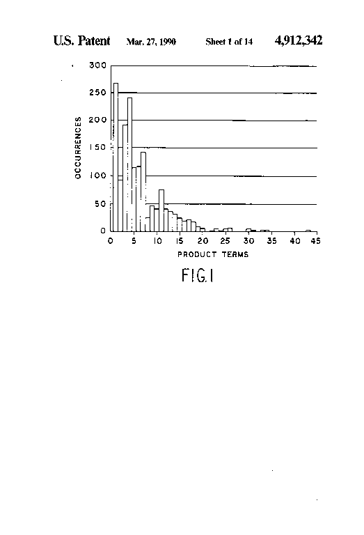
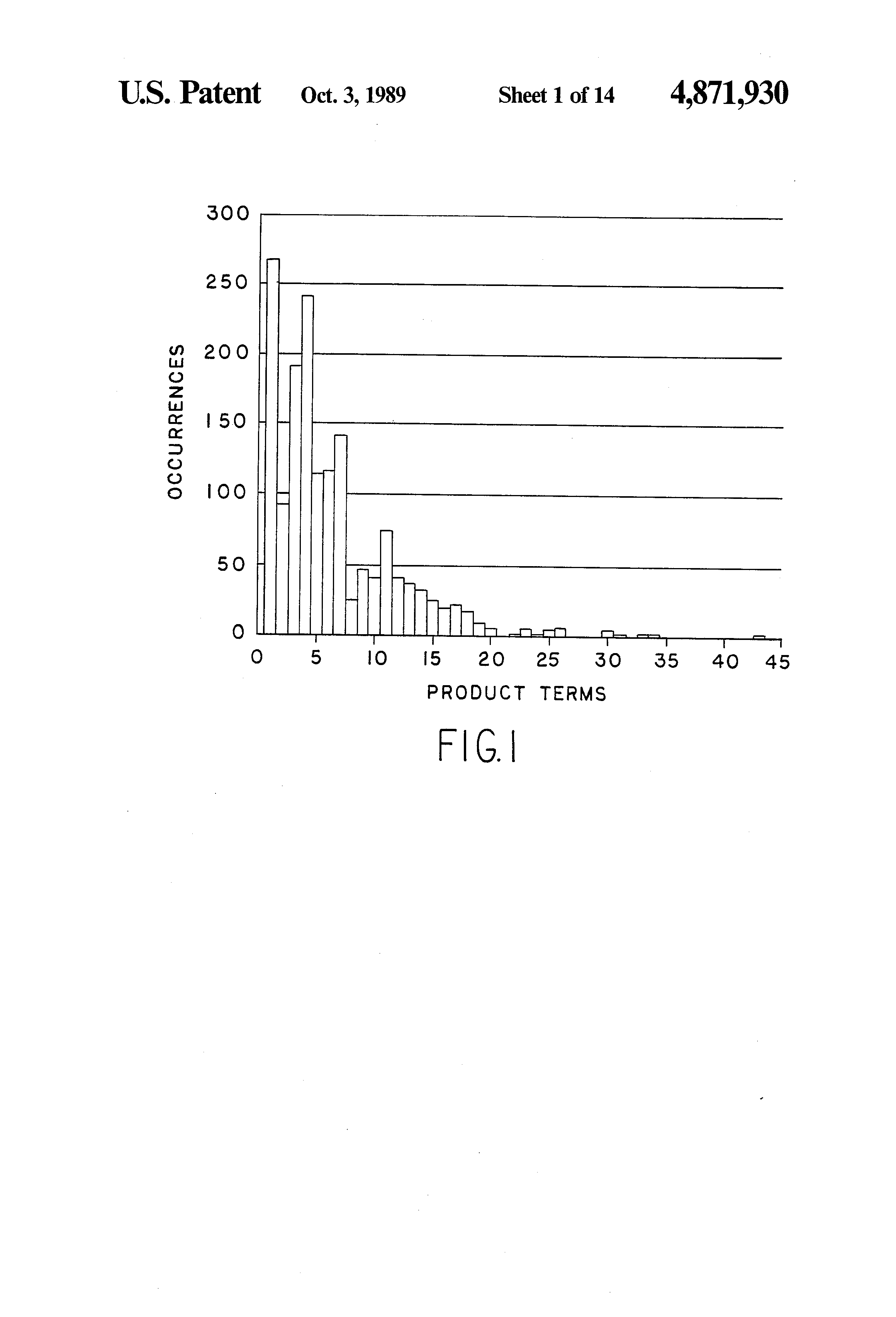
Several approaches have been used for the architecture of programmable logic integrated circuits. Among these are the "programmable AND, fixed OR" structure (referred to as a PAL) used in the above-mentioned Birkner et a. patent. This architecture has the advantages of higher speed and a simpler structure. However, because it has a fixed number of "product terms" (hereinafter "P-terms") per OR logic function (eight P-terms is typical of most current PAL products), and because these P-terms cannot be shared by neighboring OR gates, many P-terms are typically wasted. On the other hand, there are occasions when eight P-terms are not enough to handle the more complex logic functions. Experience has shown that in a broad range of applications, eight P-terms is on average much more than enough, and yet it is also often insufficient. For example, FIG. 2 in the above-mentioned Munoz et al. article is a graph of P-term requirements for a relatively large sample of logic functions (Munoz et al. FIG. 2 is substantially reproduced herein as FIG. 1). Similar studies done by the assignee of the present invention arrive at roughly similar conclusions: namely, a large percentage of logical functions (on the order of 50 to 70 percent) require less than four P-terms. However, a relatively significant "tail" exists where eight P-terms is not enough.

One way to achieve higher P-term utilization is to provide "variable P-term distribution". In essence, this is an attempt to guess a mixture of P-term requirements such that some OR gates have few P-terms (e.g., four), and some have a relatively large number (e.g., 12 or 16). See, for example, above-mentioned U.S. Pat. No. 4,609,986. This partially solves the problem of P-term utilization, but it significantly increases the complexity of the software support task because each function must be examined and then, depending upon its demand for P-term resources, assigned to a specific macrocell which has the minimum resources needed to fulfill the required demand (this process is called "fitting"). However, even with variable P-term distribution, many P-terms are typically still wasted.

Another way in which this P-term allocation problem can be solved is suggested in the above-mentioned paper by Leininger. With this structure, the P-term array is viewed as an array of programmable NOR or NAND gates whose inputs are programmable. Functions which require more than a single P-term are broken into multi-level NAND (or NOR) functions. Each level of (e.g., NAND) logic takes one P-term. Using this type of array, even quite complex logic functions can be done in a few levels of NAND logic. Again, however, there are some drawbacks. First, it is very likely that most logic functions will take more than a single P-term. This means that most often, several passes through the array will be required, and this causes a slowing down of evaluation of the function. Second, each P-term must feed back into the array input section. Thus, as the number of P-terms grows, so does the number of input lines. Even for arrays of modest complexity, the number of input signal lines (sometimes called "word lines") becomes excessive. For example, the part described in the above-mentioned IEEE ISSCC paper has only eight macrocells but has nearly 100 word lines, while a PAL circuit of similar complexity has only half as many word lines. Each word line adds to the length (and therefore the parasitic capacitance) of all of the P-terms. Greater P-term length leads to slower signal propagation.

Finally, there are programmable logic arrays ("PLAs") of the type described in the above-mentioned Spencer patent. Most (if not all) functions can be accomplished in one pass through the "AND" array plus one pass through the "OR" array. However, even the simplest functions require these two array delays. Thus, compared to the PAL architecture, there is a speed penalty (at least for simple functions). This type of PLA circuit is also more complex to execute in silicon because of the need for interface buffering between the AND and the OR array, and because of the inherently more complex programming circuits needed to program the two arrays.

In prior art programmable logic devices, a major obstacle to increasing the logic density has been array sizes which increase as the "square" of the increase in the number of output functions. This is true because for complete generality, it is necessary that all output functions also feed back as inputs into the array. However, in practice, it has been observed that this is massive overkill. That is, on average, only some subset of functions needs to be fed back. One solution to this problem is to break a single large array into several smaller arrays with functional communication between the smaller array blocks. In prior art devices such as the EP1200 (see U.S. Pat. No. 4,609,986) and the EP1800 (both commercially available from Altera Corporation of Santa Clara, Calif.), this interconnect between blocks was done in a fixed manner. That is, in a device with several array blocks, there is local feedback to an array block, and there are a certain fixed number of global feedback signals between array blocks. While this approach does serve to keep the array sub-blocks to reasonable size (both from a bit density and a speed point of view), it creates routing bottlenecks between blocks. For example, in the Altera EP1800, there are four array blocks each with 12 flip-flop macrocells. Only four macrocell outputs from each array block are routed as global inputs to the other blocks. This bottleneck causes significant restrictions in allowing logic functions to "fit" within a device even though there are enough other resources (such as flip-flops, I/O pins, etc.).

In view of the foregoing, it is an object of this invention to provide an architecture for programmable logic devices which allows for the implementation of PLDs of much greater complexity.

It is another object of the invention to maximize the utilization of P-terms in PLDs.

It is a further object of the invention to make PLDs of high complexity that can operate at high speed.

It is a further object of the invention to provide for multiple logic array blocks ("LABs") which can operate independently or in concert, and to provide for a programmable interconnect array ("PIA") structure which allows for ease of communication between these array blocks.

It is a further object of the invention to provide a macrocell which is simpler and provides for increased functionality.

It is a further object of the invention to provide a regular, repeatable architecture which will be easy for a user to understand and easy for software tools to support.

It is a further object of the invention to provide for a modular architecture which allows for ease in constructing a family of products simply by reducing or increasing the number of LABs and the associated PIA structure.

It is a further object of the invention to allow for package bonding options such that some of the I/O pins are not bonded out, thus allowing high density PLDs to be put into relatively low pin-count packages.

SUMMARY OF THE INVENTION

The present invention solves all of the above-mentioned P-term allocation problems, and in addition provides a programmable interconnect array structure which allows the implementation of much larger programmable logic devices (PLDs) than have heretofore been possible. Among the major elements of the present invention are:

1. The logic array block ("LAB") best seen in FIG. 3.

2. The macrocell/flip-flop block best seen in FIG. 5.

3. The programmable interconnect array ("PIA") best seen in FIG. 3.

4. The input/output circuit best seen in FIG. 5.

5. The clock functions best seen in FlG. 5.

( A. The Logic Array Block (LAB)

As mentioned above, the present invention increases the utilization of P-terms. Most functions (e.g., counters, demultiplexers, 2-to-1 and 4-to-1 multiplexers, and shift registers, as well as any simple AND, OR, NAND, or NOR function) can be done in one pass through the array. Many more complex functions which require three P-terms or less and which can directly utilize the EXCLUSIVE-OR (XOR) gate can also be done directly in a single pass through the array. This accounts for approximately 70% of the logic functions that are found in most logic designs. The remaining functions which require additional product terms can be done by using "expander" P-terms which (in combination with the three-P-term programmable AND, fixed OR XOR) can produce very complex NAND-NAND, AND-OR, OR-AND, and NOR-NOR types of functions. The general advantage of this combined structure is that a majority of logic functions can be done in one pass through the array (thus achieving maximum speed), and even the most complex functions can be done in two passes.

B. The Macrocell/Flip-Flop Block

The output of the above-mentioned AND-OR-XOR structure feeds a flip-flop logic block. In prior art circuits such as the Altera EP300 (see U.S. Pat. No. 4,617,479) this is typically a conventional D flip-flop with a mechanism for allowing the flip-flop register to be optionally bypassed to allow the combinational output to be applied directly to the output section if desired. In the device described herein, this structure has been modified such that the multiplexer and attendant control formerly required to bypass the flip-flop are no longer necessary. In place of the old structure a new flip-flop structure has been incorporated which allows operation as a D flip-flop, a level-sensitive latch, or a completely flow-through device which allows combinatorial functions to be directly propagated. A preferred structure for this new flip-flop is described in concurrently filed, commonly assigned, co-pending U.S. patent application Ser. No. 190,530, which is hereby incorporated by reference herein.

C. Programmable Interconnect Array (PIA)

The device of this invention solves the routing bottleneck problem by the creation of a programmable interconnect array (PIA) which allows any logic function output and any of the I/O input signals to be input to any of the logic array blocks (LABs). With this programmable interconnect array structure in place, the LABs can be kept to sizes which are functionally convenient, modular, and have a reasonable number of programmable elements. While all logic function outputs and the I/O inputs are taken into the PIA (a total of 180 word lines in the case of the device depicted in FIG. 3), only a subset (24 in the case of the present devices) are programmably routed as inputs into each of the logic array blocks. Unless an LAB requires more than 24 such inputs (which is highly unlikely), this architecture allows for completely general routing of signals.

D. Input/Output

In most prior art programmable logic devices, certain package pins are designated as inputs and others as outputs (see, for example, the MMI 16R8, commercially available from Monolithic Memories Incorporated (now merged with and part of Advanced Micro Devices ("AMD") of Sunnyvale, Calif.). An improvement on this has been the use of tri-state buffers in conjunction with a feedback path from the I/O pin back into the array such that when the output buffer is in its tri-state condition, the pin may be used as an input (see the above-mentioned Birkner et al. patent. This mechanism provides for flexibility of usage of pin resources. However, when the I/O buffer is tri-stated and the associated pin is used as an input, the associated output macrocell logic is lost. This is a waste of precious resources. A solution to this problem is provision for "dual-feedback" such as that found on certain pins of the Altera EP1800. Dual feedback provides a feedback path both from the I/O pin and from its associated logic macrocell. Thus when the output buffer is tri-stated, the I/O pin can be used as an input and the macrocell resource can still be used as a "buried" register. In the present device, this mechanism is further improved in that I/O pin feedback does not go directly into the array, but rather is an input to the PIA. Thus I/O input lines can go to any or all of the LABs, while at the same time the logic macrocell function can be used (1) locally as feedback to its own LAB, and (2) globally via the PIA. Thus I/O pin functions are effectively decoupled from the logic arrays. This provides for much greater utility and flexibility than was heretofore possible.

E. Clock Functions

Generally the register functions in PLDs are clocked either synchronously (for example, see the MMI 16R8) or asynchronously (see the MMI 20RA10). In most systems, there is a need for both types of capabilities. A solution to this problem is the structure that has been used in the Altera EP600, EP900, and EP1800. In these devices a multiplexer has been provided which allows the user to select either the synchronous (global) clock signal or an "asynchronous" (local P-term) clock. This selection can be made on a macrocell-by-macrocell basis. However, this multiplexer structure adds to the complexity of the device, and the additional circuitry needed to make the selection adds delay to the clock signal. An improved approach has been taken in the present device which allows for a simple clock gating of the "global" synchronous clock with a local P-term. If the synchronous clock is desired, then the asynchronous clock P-terms are programmed such that they are always low. This allows the global clock signal to pass to the flip-flop. If asynchronous clocking is desired, the global clock signal is forced low (again by proqramming) and the local clock P-term is allowed through to clock the flip-flop. The clock selection (i.e., synchronous versus asynchronous) is done on a per LAB basis. This structure completely eliminates the clock multiplexer and the controls for same. This new structure is simpler and faster.

Further features of the invention, its nature and various advantages will be more apparent from the accompanying drawings and the following detailed description of the invention.

BRIEF DESCRIPTION OF THE DRAWINGS

FIG. 1 is a chart showing typical product term distribution (frequency of occurrence of logic functions requiring a given number of product terms to implement the same) for a large sample of PLD designs.

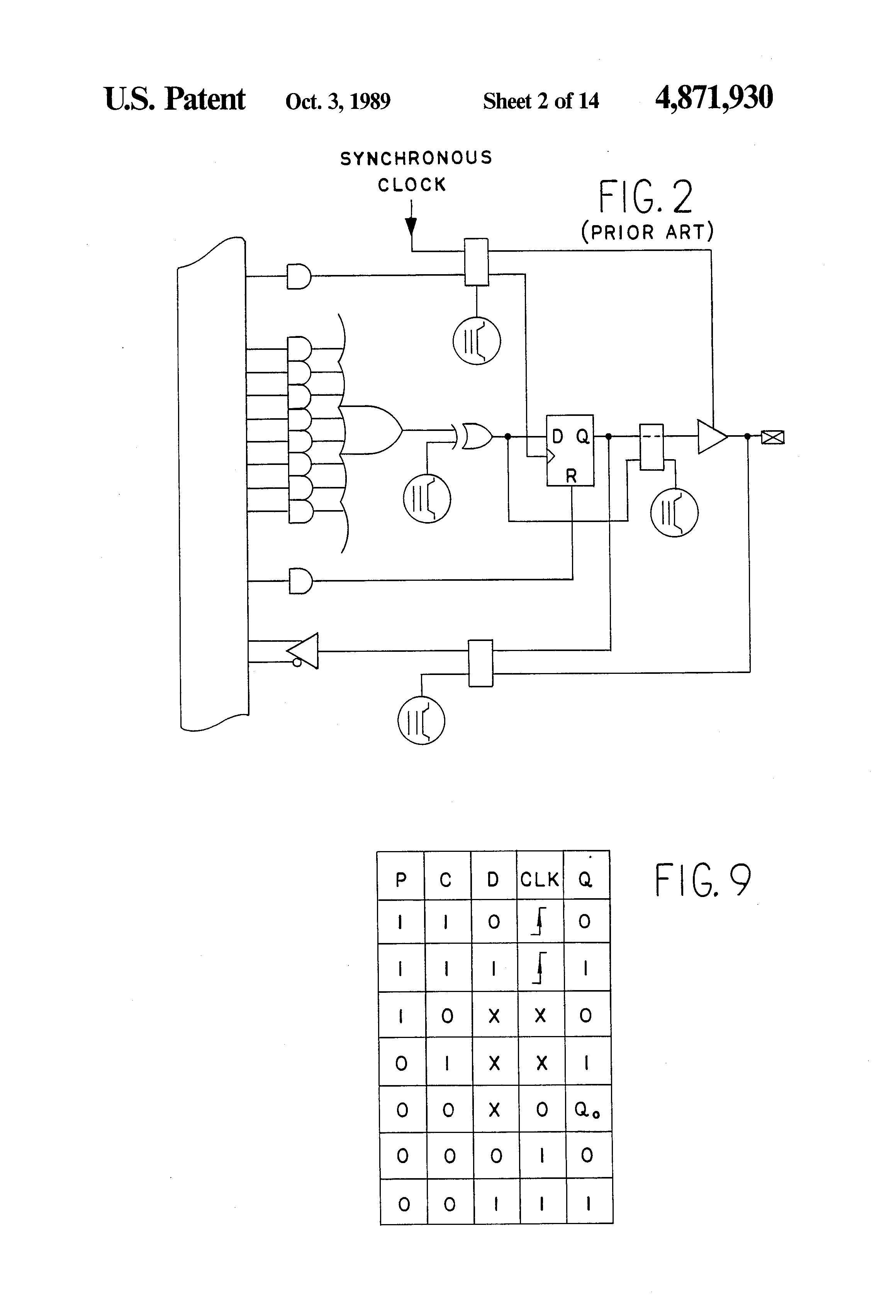
FIG. 2 is a prior art programmable logic circuit macrocell.

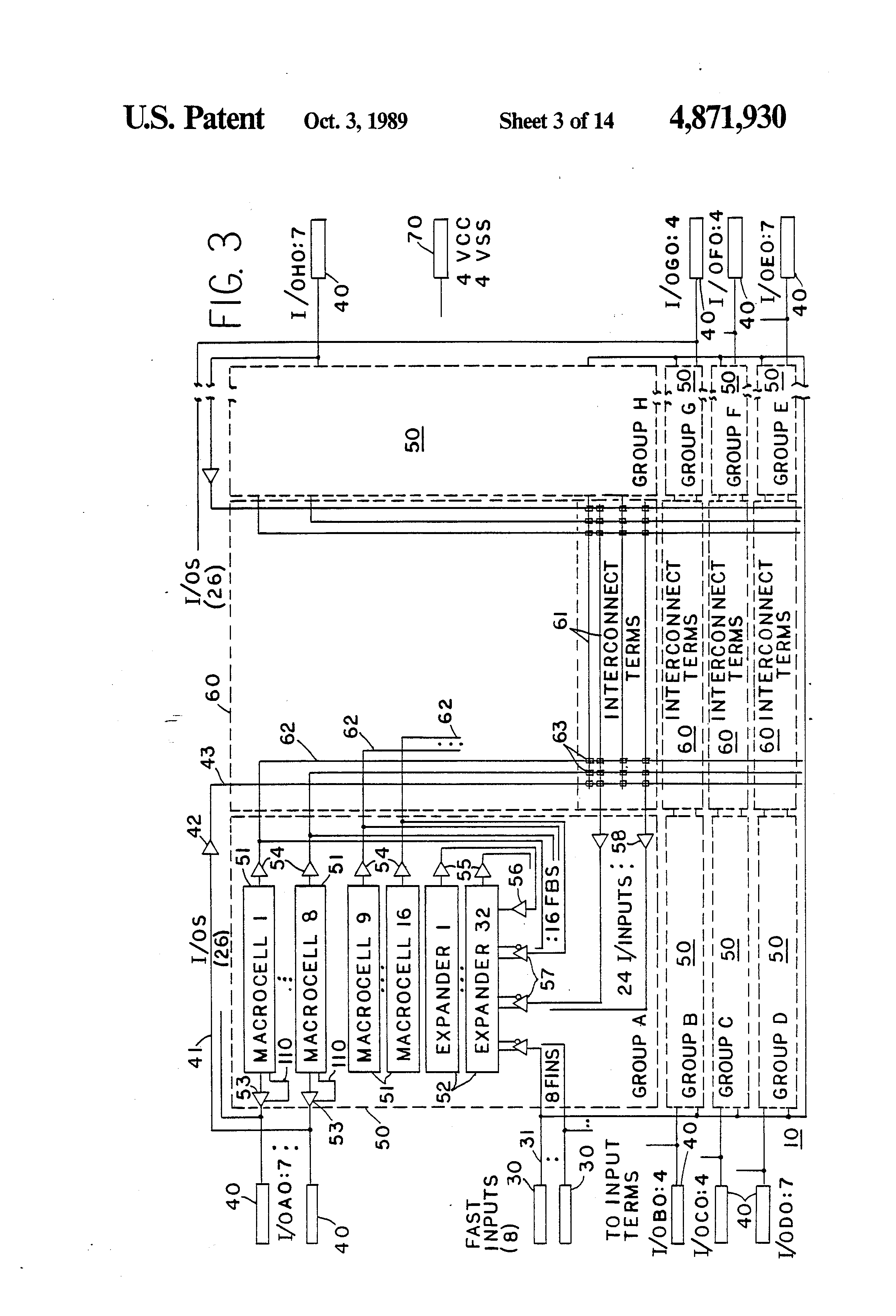
FIG. 3 is a block diagram of an illustrative embodiment of the present invention.

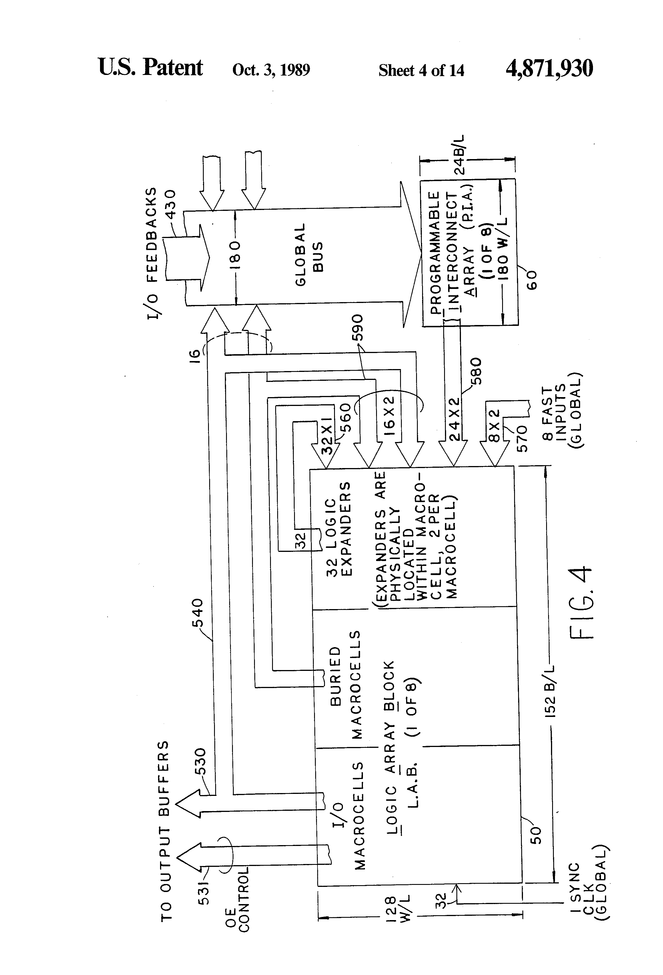
FIG. 4 is a block diagram of one section of the embodiment of FIG. 3 showing one logic array block (LAB) and one programmable interconnect array block (PIA).

FIG. 5 is a logical representation of a (macrocell) portion of an LAB in the embodiment of FIGS. 3 and 4.

FIGS. 6a (comprising parts 6a and 6aa) and 6b (comprising parts 6b and bb) are diagrams showing two "bond out options" for the device shown in block diagram form in FIG. 3.

FIG. 7 is a block diagram of an alternative embodiment having fewer LABs than the device shown in FIG. 3.

FIGS. 8a through 8h illustrate the way in which logic functions of varying complexity can be fit into the macrocell of the present invention.

FIG. 9 is a truth table useful in explaining the operation of a new flip-flop-type element used in the device of this invention.

DETAILED DESCRIPTION OF THE PREFERRED EMBODIMENTS

FIG. 3 is an overall block diagram of an illustrative embodiment of a programmable logic device 10 constructed in accordance with the present invention. The major elements shown in this diagram are "fast inputs" 30, I/O pads 40, logic array blocks (LABs) 50, and programmable interconnect array (PIA) blocks 60.

Input signals into chip 10 come from either fast inputs 30 or I/O inputs 40. Fast inputs 30 are routed via lines 31 to all of LABs 50. These signals drive into the array portion of the LAB through buffers 57 which provide both the true and complement polarity of the signal presented to the fast input pad. These lines are called fast inputs because they go directly to the LABs, in contrast to I/O inputs 40 which go indirectly to the LABs via PIA blocks 60. This can be seen by following representative signal line 41 from the pads labeled I/O0:7 (which represent eight such I/O pads) to buffer 42. After the signal has been suitably buffered by buffer 42, it drives into the PIA along line 43. By means of programmable elements 63 which are at the intersection of PIA word lines 43 and interconnect term lines 61, a signal which originated at one of the I/O pads 40 can be routed to any LAB 50 via the interconnect term 61 through buffer 58 and then into a true/complement LAB word line buffer 57. Signals propagating to an LAB via this path take additional time to traverse the PIA. Hence these signals are "slower" than the "fast" input lines 31 which go directly to the LAB as explained above. The reasons for providing these two different paths will be explained in due course.

A typical LAB 50 will now be explained in more detail. In this architecture there can be as many LABs as is deemed desirable. For example, in various preferred embodiments implemented to date we have used either four or eight LABs.

Each LAB 50 comprises macrocells 51 and expanders 52. Inputs to the LAB are provide by fast inputs via buffers 57, PIA inputs via interconnect terms 61 through buffers 58 and 57, feedback terms from macrocell outputs via buffers 54 and 57, and expander feedback terms via buffers 55 and 56. Two types of macrocells are provided. The only difference is the inclusion of output buffers 53 (plus their associated output enable (OE) signal 110 which provides the output tri-state control) in macrocells 1 through 8. Output buffers 53 selectively apply the associated macrocell outputs to I/O signal pins 40. Macrocells 9 through 16 have no associated output buffer and are therefore sometimes referred to as "buried" macrocells. In either case, the macrocells all have buffers 54 which take the signal generated by the macrocell and feed it to its own LAB (as described above) and also drive PIA word lines 62.

In the preferred embodiment shown in FIG. 3, each LAB 50 has 16 macrocells, 32 expanders, eight fast inputs, and 24 array inputs from the interconnect terms of the PIA. Each LAB also has a number of tri-state output drivers 53: eight drivers 53 in the case of the LABs labelled group A, B, H, and G, and five drivers 53 in the case of the LABs labelled group C, D, F, and E. While we believe these choices to be optimum for the particular embodiment shown, other choices could be made without departing from the scope and spirit of the invention. For example, in another embodiment (shown in FIG. 7), there are four LABs, each of which.. has seven tri-state drivers. In addition, the chip shown in FIG. 7 has eight dedicated inputs and four power/ground pins.

PIA blocks 60 will now be described with reference to FIG. 3. The PIA provides a mechanism for programmably routing signals from I/O input pins 40 to any LAB and from any LAB macrocell output to any other LAB. The PIA includes word lines 43 and 62 and bit lines 61. The bit lines are also labelled "interconnect terms" in FIG. 3. In the preferred embodiment shown, there are 52 word lines 43 which come from the I/O lines, and there are 128 word lines 62 which are driven from macrocell buffers 54. Interconnect terms 61 are perpendicular to the word lines. At the intersections of the word lines and bit lines are programmable elements 63 which, when programmed in one state, provide a connection between the associated word and bit lines, and which, when programmed in the other state, provide no such connection. In the preferred embodiment, the programmable elements are EPROM transistors. However, other types of programmable elements such as EEPROM transistors, fuses, anti-fuses, or other similar elements could be used without departing from the scope and spirit of the invention. There are 24 interconnect terms 61 feeding each LAB 50 in the embodiment shown. Again, this number is an estimate as to the optimum number for the device shown in FIG. 3, but a larger or smaller number could be used if desired. The entire PIA (i.e., all of PIA blocks 60 taken together) is therefore a programmable array with 180 word lines and 192 bit lines (eight groups of 24 bit lines).

FIG. 4 is a block diagram showing a singe LAB 50 and its associated PIA 60. This diagram shows, in concept, the signal routing to and from the LAB and the PIA. Lines going into the LAB are the fast inputs 570 shown as a group of 8×2=16 lines (true and complement signals), the interconnect terms 580 shown as a group of 24×2=48 lines (true and complement signals), the macrocell feedback lines 590 shown as two groups totaling 16×2=32 lines (true and complement signals), and the "expander" feedback lines 560 shown as a group of 32 lines (single polarity only). This totals to 128 word lines for each LAB in the embodiment shown. There are 152 bit lines (P-terms) in each LAB. These will be described in detail in the discussion of FIG. 5. Shown in the diagram of FIG. 4 are the groups of signals 530 and 531 going to the output buffers labeled 53 in FIG. 3. Lines 530 provide the path for data from the macrocells to the output buffers, and lines 531 provide the path for the output enable (OE) signals from the OE P-terms. The PIA block 60 associated with this LAB is shown as having 180 word lines and 24 bit lines as previously described.

Referring now to FIG. 5, we can see more of the detail of one of the macrocells. In this case it is shown with an I/O buffer 53. If it were a buried macrocell, the only difference (at least pictorially) would be the absence of output buffer 53, the OE P-term structure (101, 103, 110), and I/O pin 40. The programmable array is shown as the intersection of word lines 102 and bit lines 101. The label 51 refers to that part labelled "macrocell" in FIG. 3, and the label 52 refers to that part labelled "expander" in FIG. 3. Actually, in the physical layout of the chip, two expander P-terms are preferably grouped with the P-terms of each: macrocell for convenience. In the description of FIG. 5, the word "macrocell" will be used to describe the entire collection of P-terms (including the two expander P-terms) and the associated logic gates 103-107, flip-flop 123, and output buffer 53, if present.

There are ten P-terms 101 in this macrocell. Each P-term receives inputs from the 128 word lines 102 (described earlier). There is a programmable element (similar to element 63 in the PIA) at the intersection of each bit line with each word line. A logical AND function of any of the word line variables can be formed by programming; these elements. This is described in U.S. Pat. No. 4,617,479 and will not be repeated here. The correct logical outcome produced by each P-term is represented either as an active-low AND gate 103 or as a NOR gate 104. Those skilled in the art will recognize that other representations could be shown without departing from the scope and spirit of the invention. For example, an active-high AND gate could be used if one notes that the opposite polarity word line were used as its input and thus achieve the same logical result.

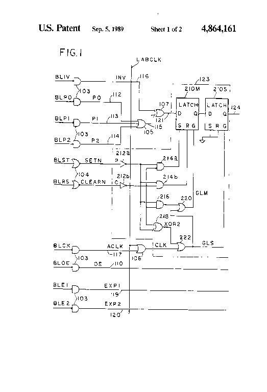
The purpose of each P-term is as follows: The P-term labelled OE is used as the output enable for the associated output buffer 53. If this were a buried macrocell, this bit line would be absent. SETN is used to control the preset of flip-flop 123. The next three terms, P0, P1, and P2, feed OR gate 105 which produces alogical sum-of-products at its output 115. This collection of P-terms, in conjunction with gate 105, forms the "programmable AND, fixed OR" function described in U.S. Pat. No. 4,124,899. The term labeled INV is used as an "invert control" for XOR gate 107. This allows for the creation of inverted sum-of-product functions at line 121. This will be recognized by those skilled in the art as expanding the number of possible functions which can be realized. In addition to acting as a static control for the inverted sum-of-products option, the INV term can be used "dynamically" as a direct input to the XOR gate 107. For example, any logic function which can be reduced to (1) an EXCLUSIVE-OR of an AND function with an AND-OR function, (2) an EXCLUSIVE-OR of an OR function with an OR-AND function, (3) an EXCLUSIVE-OR of an OR function with an AND-OR function, or (4) and EXCLUSIVE-OR of an AND function with an OR-AND function can be implemented directly in one pass through the array. (This is shown in detail in FIGS. 8a and 8c; the dollar sign in FIG. 8a represents the EXCLUSIVE-OR function.) ACLK is used to create an "asynchronous" clock signal for flip-flop 123 in conjunction with gate 106 and gates 109 and 108. CLEARN is used to control the "Clear" line on flip-flop 123. EXP1 and EXP2 are the "expander" P-terms. Note that each expander 52 preferably includes only a single P-term.

Our assignee has studied the most often used logic functions in relation to a variety of possible architectures. In particular, the AND-OR-XOR structure of P0, Pl, P2, OR gate 105, and XOR gate 107 was analyzed assuming both less than three AND P-terms (e.g., two AND P-terms) feeding OR gate 105, and more than three AND P-terms (up to eight P-terms such as is used in the prior art macrocell of FIG. 2) feeding the OR gate. The classes of functions included the following: adders, comparators, counters, decoders, demultiplexers, parity generators, and shift registers. The purpose of the study was to evaluate the architecture of the present invention relative to the prior art architecture of FIG. 2. The present new architecture is a combination of three programmable ANDs, a fixed OR, and an XOR, with single-P-term "expanders". This architecture is believed to be superior to both the prior art structure shown in FIG. 2 and to the single-P-term architectures proposed in the above-mentioned Goetting et al. reference. The study bore this out and reached several other important conclusions. It was found that having less than three P-terms feeding the OR gate is very restrictive when doing counters and shift registers. For all other functions examined, three P-terms feeding the OR gate was always as good as four P-terms feeding the OR. (This is only true assuming that in either case there is the additional BLIV P-term and XOR gate 107.) The prior art eight-P-term architecture is only superior for a very limited group of functions (for example, multiplexers with more than four inputs). The study also demonstrated that having approximately two expander P-terms per macrocell was more than sufficient to accommodate the less common functions which require many P-terms.

Expanders 52 play an important role in this new architecture. As their name implies, these P-terms allow for growth. That is, they allow for implementation of those (less common) functions which do not fit within the three-P-term limit (for example, an 8-to-1 multiplexer can be fit into 9 expanders). Expander P-terms anywhere in the LAB can be used to form elements of these more complex functions, and then the outputs of these P-terms are combined using another P-term (typically one of the P-terms feeding a fixed OR gate 105) (see, for example, FIG. 8f). Functions formed with expander p-terms can also be used to feed other expanders on single p-terms such as INV, ACLK, SETN, CLEARN, or OE. Also, there are often common P-terms which can be used by a number of logic functions. These common P-terms can be formed by the expanders and then fed to those functions (which are likely to be implemented in a programmable AND, fixed OR section) for which they are required. FIG. 8e shows an example of a logic expression which requires more than three P-terms which can be factored into expressions which can be formed using the expander P-terms and recombined using another P-term (typically this will be a P-term which feeds the fixed OR gate). In FIG. 8e, the original expression has been factored such that two factors are implemented in two expanders and then combined with the remainder of the expression in one of the P-terms feeding the fixed OR rate. The original expression was:

This expression can be factored and rewritten as:

The common factors X*Y are formed on the P-term feeding he fixed OR gate, while the remaining factors (A+B+C) and (D+E) are formed on each of two expanders and fed to the P-term which contains the X*Y term. In this example, an expression which would have required six P-terms to implement can now be done in three P-terms. Suppose further that either the expression (A+B+C) or the expression (D+E) were required by some other macrocell or macrocells. These same expressions formed on the expander P-terms could be used again by those other macrocells. Thus an expression generated on the expanders can be amortized across all of the macrocells which have the expander's outputs as word line inputs. This again results in an overall saving of valuable P-term resources. Examples of various types of logic functions which can be fit into the P-term structure of the present invention are shown in FIGS. 8a through 8g. Latches require only two expanders. This structure is shown in FIG. 8h.

Continuing now with FIG. 5, XOR gate 107 receives its inputs from OR gate 105 and P-term INV. Those skilled in the art will recognize that if the logic signal on line 116 is 0, then the output of XOR gate 107 (line 121) will have the same logic value as input 115. On the other hand if line 116 is 1, then 121 will be the logical inversion of 115. In addition to allowing for inverted sum-of-product functions, or positive or inverted product-of-sum functions, this structure, in conjunction with a D flip-flop such as 123, also allows for emulating other flip-flop types such as T, J-K, and R-S. Emulation of various flip-flop types using array logic and XOR gates is the subject of U.S. Pat. No. 4,677,318. When using the expander P-terms as an AND array and the P-terms feeding the OR gate 105 as an OR array, the INV signal 116 needs to be set to a logic 1.

Flip-flop block 123 appears to be a simple D flip-flop with active low preset (P) and clear (C). However, this is done for simplicity of illustration of the macrocell. FIG. 9 is a truth table which explains the full functionality of element 123. Note that if P=C=1, then 123 is an edge-triggered flip-flop. At the rising edge of CLK (line 122 in FIG. 5), whatever data is present at the D input 121 is transferred to the Q output 124. If P is 0 and C is 1, then the Q output will be forced to 1 independent of the state of CLK or D. If C is 0 and P is 1, then the Q output will be forced to 0 independent of the state of CLK or D. To those skilled in the art, the case where P=C=0 is an illegal condition and is not defined. For flip-flop 123, however, when P=C=0, the flip-flop is redefined as shown in FIG. 9. It thus becomes a "flow-through latch". Then, whenever line 122 is high, the Q output takes the value of whatever is on the D input. Whenever line 122 is low, the Q output holds the value that was present at the D input when line 122 went low. If line 122 is held high (for example, by programming P-term ACLK high), then signals will propagate directly from 121 to 124. This is the same "combinatorial" function as was provided by multiplexers and architectural control EPROM bits on prior art EPLD circuits. The present new design is simpler, faster, and provides greater functionality. As has been mentioned, a preferred structure for implementing flip-flop 123 is shown in concurrently filed, commonly assigned, co-pending patent application Ser. No. 190,530, which is hereby incorporated by reference herein.

The output signal 124 from flip-flop 123 (1) goes to the input of output driver 53, (2) feeds back (via buffer 54) to a word line driver 57 of its own LAB, and (3) drives one of the word lines of the PIA (indicated as line 62 in FIG. 3) This signal 124 can be used by any other LAB via iLs connection through the PIA. The signal also feeds a conventional tri-state I/O buffer 53 such that if the buffer is enabled by line 110, the signal from 124 will drive off chip through I/O pin 40. I/O pin 40 can also provide an input path from off chip via line 41. This line drives buffer 42 (FIG. 3) whose output becomes one of the word lines for the PIA shown as line 43 in FIG. 3. I/O buffer 53 can be dynamically controlled by the OE P-term, in which case pin 40 may be both an input and an output depending upon the state of line 110. Alternatively, by programming the chip such that OE is always 0, buffer 53 will always be disabled, in which case I/O pin 40 can be used permanently as an input. Thus each of I/O pins 40 can be configured as input, output, or bi-directional input/output terminals. Because of the feedback of signal 124 to the LAB and the PIA, and the I/O input line 41, disabling of the output driver 53 does not result in the loss of the macrocell's functionality. This is a significant advantage over some prior art devices.

Turning now to the clock structure for the LAB, this structure includes inverter 109, AND gate 108, OR gate 106, and P-term ACLK. Three modes of operation are anticipated as follows:

COMBINATORIAL MODE: In this case, P=C=0 as previously described. Further, the ACLK P-term is programmed to always be 1, and line 122 is therefore also always 1. Whatever data is present at line 121 will pass through flip-flop 123 and appear at line 124.

ASYNCHRONOUS MODE: In this case, the line labeled ECKN (which is an extra P-term (not shown) in the LAB) is programmed to be 1. This means that line 125 is logic 0. Then line 122 is directly controlled by the state of the ACLK P-term. ACLK can be any (inputs active-low) AND function of any of the word line variables. Each flip-flop in the LAB has its own separate ("asynchronous") P-term clock.

SYNCHRONOUS MODE: P-term ACLK is programmed to be always 0. Also, ECKN is programmed ed to be 0 and thus ECK is 1. This allows the signal EXT.(SYNC.) CLK. on line 32 to propagate through AND gate 108 and appear on line 125. EXT.(SYNC.)CLK. line 32 comes from an input pad (one of the "fast inputs") not shown. This signal on line 125 passes through OR gate 106 and appears on line 122. In this way, an external signal can directly control the clocking of flip-flop 123. Because there is a single ECKN P-term per LAB, the selection of synchronous mode is done on a per LAB basis rather than on a per macrocell basis.

Another advantage of the chip architecture of the present invention is that chips of any given configuration can be packaged in any of a variety of ways with no loss of internal resources. For example, FIG. 6a illustrates one way in which the chip of FIG. 3 can be bonded out to 68 pins, while FIG. 6b shows how the same chip can be bonded out to 40 pins. The chip pads which are not bonded out in FIG. 6b are certain I/O pins. However, the "output" signals that could be applied to these chip pads are still usable internally, and the remaining external inputs can be applied to any-LAB via PIA 60. Thus, even though some chip pads are not bonded out in FIG. 6b, the only loss in chip capability is the loss of the external chip I/O connections. (With reference to FIGS. 6a and 6b, the eight LABs on the chip are designated A through H. Thus, for example, in FIG. 6a eight I/O pads 1/OA0-8 of LAB A are bonded out to lead tips 11 through 4, respectively while in FIG. 6b only four I/O pads I/OA0, 1, 2, and 7 are bonded out to lead tips 37 through 34, respectively. In FIG. 6a LABs A, D, E, and H each have eight bonded-out I/O pads and the remaining LABs each have five bonded-out I/O pads. In FIG. 6b LABs A, D, E, and H each have four bonded-out I/O pads and the remaining I/O pads each have three-bonded out I/O pads. In both FIG. 6a and 6b the "fast" inputs are designated IO through I7.)

Although particular numbers of such components as macrocells, expanders, fast inputs, and array inputs from the PIA are employed in the depicted embodiments described above, it will be understood that (among other possible variations within the scope of the invention that will occur to those skilled in the art) any number of such components can be used without departing from the scope and spirit of the invention.
Claims (15)

  1. A programmable logic device for producing a plurality of first signals, each of which is a programmable logical function of a plurality of second signals, each of which is applied to a respective one of a plurality of word line conductors, said programmable logic device comprising: a plurality of first P-term line conductors, each of which is programmably interconnectable to each of said word line conductors for producing on each of said first P-term line conductors a third signal which is a logical function of the second signals applied to the word line conductors to which that first P-term line conductor is interconnected; means for logically combining said third signals to produce a first of said first signals; at least one second P-term line conductor which is programmably interconnectable to each of said word line conductors for producing on said second P-term line conductor a second of said first signals which is a logical function of the second signals applied to the word line conductors to which said second P-term line conductor is interconnected; and means for applying said second of said first signals to one of said word line conductors as the second signal applied to that word line conductor, wherein said first and second P-term line conductors comprise a macrocell, and wherein said apparatus includes a plurality of said macrocells, said word line conductors being common to all of said macrocells.
  2. The apparatus defined in claim 1 wherein the number of macrocells in said apparatus is greater than the number of said first P-term line conductors in any one of said macrocells.
  3. The apparatus defined in claim 1 wherein the total number of said second P-term line conductors in said apparatus is greater than the number of first P-term line conductors in any one of said macrocells.
  4. The apparatus defined in claim 1 wherein in any one macrocell, the number of said first P-term line conductors is greater than the number of said second P-term line conductors.
  5. The apparatus defined in claim 1 wherein each of said first and second P-term line conductors is programmably interconnectable to each of said word line conductors via a programmable element selected from the group consisting of an EPROM transistor and an EEPROM transistor.
  6. A programmable logic device comprising: first and second logic array blocks respectively including (1) separate first and second pluralities of word line conductors; (2) separate first and second pluralities of P-term line conductors, each of said P-term line conductors in said first plurality of P-term line conductors being programmably interconnectable only to each of said word line conductors in said first plurality of word line conductors, and each of said P-term line conductors in said second plurality of P-term line conductors being programmably interconnectable only to each of said word line conductors in said second plurality of word line conductors, for producing on each P-term line conductor a signal which is a logical function of the signals on the word line conductors to which that P-term line conductor is interconnected; and (3) separate first and second means for respectively deriving a first output signal from at least one of said P-term line conductor signals associated with said first plurality of P-term line conductors and a second output signal from at least one of said P-term line conductor signals associated with said second plurality of P-term line conductors; and programmable means for selectively applying said first output signal to at least one of the word line conductors in said second plurality of word line conductors.
  7. The apparatus defined in claim 6 further comprising: means for applying the output signal of said at least one logic array block to at least one of the word line conductors of said at least one logic array block.
  8. The apparatus defined in claim 6 wherein at least one of said P-term line conductors signals in at least one of said logic array blocks is applied to at least one of the word line conductors of that logic array block and only that logic array block.
  9. The apparatus defined in claim 6 wherein at least one of said P-term line conductor signals in at least one of said logic array blocks is applied only to one of the word line conductors of that logic array block.
  10. The apparatus defined in claim 6 further comprising: means for receiving an input signal applied to the programmable logic device; and programmable means for selectively applying said input signal to at least one of the word line conductors of at least one of said logic array blocks.
  11. The apparatus defined in claim 6 further comprising: means for receiving an input signal applied to the programmable logic device; and programmable means for, selectively applying said input signal to at least one of the word line conductors of either or both of said logic array blocks.
  12. The apparatus defined in claim 6 wherein each of said P-term line conductors in each of said first and second logic array blocks is programmably interconnectable to each of said wordline conductors in the associated logic array block via a programmable element selected from the group consisting of an EPROM transistor and an EEPROM transistor.
  13. The apparatus defined in claim 6 wherein said programmable means comprises a programmable element selected from the group consisting of an EPROM transistor and an EEPROM transistor.
  14. The apparatus defined in claim 10 wherein said programmable means for selectively applying said input signal to at least one of the word line conductors of at least one of said logic array blocks comprises a programmable element selected from the group consisting of an EPROM transistor and an EEPROM transistor.
  15. The apparatus defined in claim 11 wherein said programmable means for selectively applying said input signal to at least one of the word line conductors of either or both of said logic array blocks comprises a programmable element selected from the group consisting of an EPROM transistor and an EEPROM transistor.

Publications

Related applications (7)

  1. US07/190,663

    Priority application

  2. DE68919117T

    Priority application

  3. EP89301780A

    Priority application

  4. JP1112328A

    Priority application

  5. US07/407,411

    Priority application

  6. US07/190,663

    Claims priority

  7. US07/190,663

    Patent family

Record timeline

  1. Application filed by Altera Corp

  2. Assigned to ALTERA CORPORATION, A CORP. OF CA

  3. Priority to US07/190,663

  4. Priority to DE68919117T

  5. Priority to EP89301780A

  6. Priority to JP1112328A

  7. Priority to US07/407,411

  8. Publication of US4871930A

  9. Application granted

  10. Assigned to ALTERA CORPORATION (A CORPORATION OF DELAWARE)

  11. Assigned to ALTERA CORPORATION, A DELAWARE CORPORATION

  12. Anticipated expiration

  13. Expired - LifetimeCurrent

Legal events

  1. AS

    Assignment

    Owner name: ALTERA CORPORATION, A CORP. OF CA,CALIFORNIA

    Free format text: ASSIGNMENT OF ASSIGNORS INTEREST;ASSIGNORS:WONG, SAU-CHING;SO, HOCK-CHUEN;KOPEC, STANLEY J. JR.;AND OTHERS;REEL/FRAME:004881/0919

    Effective date: 19880504

    Owner name: ALTERA CORPORATION, 3525 MONROE STREET, SANTA CLAR

    Free format text: ASSIGNMENT OF ASSIGNORS INTEREST.;ASSIGNORS:WONG, SAU-CHING;SO, HOCK-CHUEN;KOPEC, STANLEY J. JR.;AND OTHERS;REEL/FRAME:004881/0919

    Effective date: 19880504

  2. STCF

    Information on status: patent grant

    Free format text: PATENTED CASE

  3. FEPP

    Fee payment procedure

    Free format text: PAYOR NUMBER ASSIGNED (ORIGINAL EVENT CODE: ASPN); ENTITY STATUS OF PATENT OWNER: LARGE ENTITY

    Free format text: PAT HLDR NO LONGER CLAIMS SMALL ENT STAT AS SMALL BUSINESS (ORIGINAL EVENT CODE: LSM2); ENTITY STATUS OF PATENT OWNER: LARGE ENTITY

  4. FPAY

    Fee payment

    Year of fee payment: 4

  5. FPAY

    Fee payment

    Year of fee payment: 8

  6. AS

    Assignment

    Owner name: ALTERA CORPORATION (A CORPORATION OF DELAWARE), CA

    Free format text: MERGER;ASSIGNOR:ALTERA CORPORATION (A CORPORATION OF CALIFORNIA);REEL/FRAME:008811/0577

    Effective date: 19970618

  7. AS

    Assignment

    Owner name: ALTERA CORPORATION, A DELAWARE CORPORATION, CALIFO

    Free format text: MERGER;ASSIGNOR:ALTERA CORPORATION, A CALIFORNIA CORPORATION;REEL/FRAME:009015/0336

    Effective date: 19970325

  8. FPAY

    Fee payment

    Year of fee payment: 12

Patent citations (14)

  1. US3566153A

    Programmable sequential logic

    Texas Instruments Inc · February 23, 1971 · Examiner cited

  2. US4124899B1

    April 28, 1987 · Examiner cited

  3. US4124899A

    Programmable array logic circuit

    Monolithic Memories, Inc. · November 7, 1978 · Examiner cited

  4. US4525641A

    Flip-flop programmer using cascaded logic arrays

    International Business Machines Corporation · June 25, 1985 · Examiner cited

  5. US4554640A

    Programmable array logic circuit with shared product terms

    Monolithic Memories, Inc. · November 19, 1985 · Examiner cited

  6. US4617479A

    Programmable logic array device using EPROM technology

    Altera Corporation · October 14, 1986 · Examiner cited

  7. US4617479B1

    Programmable logic array device using eprom technology

    Altera Semiconductor Corp. · September 21, 1993 · Examiner cited

  8. US4609986A

    Programmable logic array device using EPROM technology

    Altera Corporation · September 2, 1986 · Examiner cited

  9. US4677318A

    Programmable logic storage element for programmable logic devices

    Altera Corporation · June 30, 1987 · Examiner cited

  10. US4689654A

    Logic array chip

    Nixdorf Computer Ag · August 25, 1987 · Examiner cited

  11. US4713792A

    Programmable macrocell using eprom or eeprom transistors for architecture control in programmable logic circuits

    Altera Corporation · December 15, 1987 · Examiner cited

  12. US4758746A

    Programmable logic array with added array of gates and added output routing flexibility

    Monolithic Memories, Inc. · July 19, 1988 · Examiner cited

  13. US4664191A

    Minimizing formation damage during gravel pack operations

    Mobil Oil Corporation · May 12, 1987 · Examiner cited

  14. US4703206A

    Field-programmable logic device with programmable foldback to control number of logic levels

    Signetics Corporation · October 27, 1987 · Examiner cited

Non-patent citations (6)

  1. E. Goetting et al., "A CMOS Electrically-Reprogrammable ASIC with Multi-Level Random Logic Capabilities," 1986 IEEE International Solid-State Circuits Conference, pp. 244-245 and 359-360, 1986.
  2. E. Goetting et al., A CMOS Electrically Reprogrammable ASIC with Multi Level Random Logic Capabilities, 1986 IEEE International Solid State Circuits Conference, pp. 244 245 and 359 360, 1986.
  3. J. C. Leininger, "Universal Logic Module," IBM Technical Disclosure Bulletin, vol. 13, No. 5, pp. 1294-1295, Oct. 1970.
  4. J. C. Leininger, Universal Logic Module, IBM Technical Disclosure Bulletin, vol. 13, No. 5, pp. 1294 1295, Oct. 1970.
  5. R. R. Munoz et al., "Automatic Partitioning of Programmable Logic Devices," VLSI Systems Design, Oct. 1987, pp. 74-76, 78, and 86.
  6. R. R. Munoz et al., Automatic Partitioning of Programmable Logic Devices, VLSI Systems Design, Oct. 1987, pp. 74 76, 78, and 86.

Cited by (395)

  1. US5764078A

    Family of multiple segmented programmable logic blocks interconnected by a high speed centralized switch matrix

    Advanced Micro Devices, Inc. · June 9, 1998 · Examiner cited

  2. US5869981A

    High density programmable logic device

    Advanced Micro Devices, Inc. · February 9, 1999 · Examiner cited

  3. US5612631A

    An I/O macrocell for a programmable logic device

    Advanced Micro Devices, Inc. · March 18, 1997 · Examiner cited

  4. US5436514A

    High speed centralized switch matrix for a programmable logic device

    Advanced Micro Devices, Inc. · July 25, 1995 · Examiner cited

  5. US5426335A

    Pinout architecture for a family of multiple segmented programmable logic blocks interconnected by a high speed centralized switch matrix

    Advanced Micro Devices, Inc. · June 20, 1995 · Examiner cited

  6. US5606267A

    Programmable logic module and architecture for field programmable gate array device

    Actel Corporation · February 25, 1997 · Examiner cited

  7. US5698992A

    Programmable logic module and architecture for field programmable gate array device

    Actel Corporation · December 16, 1997 · Examiner cited

  8. US5570041A

    Programmable logic module and architecture for field programmable gate array device

    Actel Corporation · October 29, 1996 · Examiner cited

  9. US5510730A

    Reconfigurable programmable interconnect architecture

    Actel Corporation · April 23, 1996

  10. US5781033A

    Logic module with configurable combinational and sequential blocks

    Actel Corporation · July 14, 1998 · Examiner cited

  11. US5610534A

    Logic module for a programmable logic device

    Actel Corporation · March 11, 1997 · Examiner cited

  12. US5349691A

    Programming process for 3-level programming logic devices

    Xilinx, Inc. · September 20, 1994 · Examiner cited

  13. US6078191A

    Programmable application specific integrated circuit and logic cell

    Quicklogic Corporation · June 20, 2000 · Examiner cited

  14. US5986468A

    Programmable application specific integrated circuit and logic cell therefor

    Quicklogic Corporation · November 16, 1999 · Examiner cited

  15. US5594364A

    Programmable application specific integrated circuit and logic cell therefor

    Quicklogic Corporation · January 14, 1997 · Examiner cited

  16. US5587669A

    Programmable application specific integrated circuit and logic cell therefor

    Quicklogic Corporation · December 24, 1996 · Examiner cited

  17. US5726586A

    Programmable application specific integrated circuit and logic cell therefor

    Quicklogic Corporation · March 10, 1998 · Examiner cited

  18. US5220214A

    Registered logic macrocell with product term allocation and adjacent product term stealing

    Altera Corporation · June 15, 1993 · Examiner cited

  19. US5861760A

    Programmable logic device macrocell with improved capability

    Altera Corporation · January 19, 1999 · Examiner cited

  20. US5384499A

    High-density erasable programmable logic device architecture using multiplexer interconnections

    Altera Corporation · January 24, 1995 · Examiner cited

  21. US6366119B1

    Programmable logic device macrocell with improved logic capability

    Altera Corporation · April 2, 2002

  22. US6707315B2

    Registered logic macrocell with product term allocation and adjacent product term stealing

    Altera Corporation · March 16, 2004

  23. US5241224A

    High-density erasable programmable logic device architecture using multiplexer interconnections

    Altera Corporation · August 31, 1993 · Examiner cited

  24. US5557217A

    High-density erasable programmable logic device architecture using multiplexer interconnections

    Altera Corporation · September 17, 1996 · Examiner cited

  25. US5268598A

    High-density erasable programmable logic device architecture using multiplexer interconnections

    Altera Corporation · December 7, 1993 · Examiner cited

  26. US6157208A

    Programmable logic device macrocell with improved logic capability

    Altera Corporation · December 5, 2000 · Examiner cited

  27. US5598108A

    High-density erasable programmable logic device architecture using multiplexer interconnections, and registered macrocell with product term allocation and adjacent product term stealing

    Altera Corporation · January 28, 1997 · Examiner cited

  28. US5485103A

    Programmable logic array with local and global conductors

    Altera Corporation · January 16, 1996 · Examiner cited

  29. US6759870B2

    Programmable logic array integrated circuits

    Altera Corporation · July 6, 2004

  30. US5517186A

    EPROM-based crossbar switch with zero standby power

    Altera Corporation · May 14, 1996 · Examiner cited

  31. US5357144A

    Complementary logic circuit

    Sony Corporation · October 18, 1994 · Examiner cited

  32. US5633806A

    Semiconductor integrated circuit and method of designing same

    Mitsubishi Denki Kabushiki Kaisha · May 27, 1997 · Examiner cited

  33. US5485102A

    Programmable logic devices with spare circuits for replacement of defects

    Altera Corporation · January 16, 1996 · Examiner cited

  34. US5498975A

    Implementation of redundancy on a programmable logic device

    Altera Corporation · March 12, 1996 · Examiner cited

  35. US5463328A

    Expanded programmable logic architecture

    Altera Corporation · October 31, 1995 · Examiner cited

  36. US5483178A

    Programmable logic device with logic block outputs coupled to adjacent logic block output multiplexers

    Altera Corporation · January 9, 1996 · Examiner cited

  37. US5350954A

    Macrocell with flexible product term allocation

    Altera Corporation · September 27, 1994 · Examiner cited

  38. US5473266A

    Programmable logic device having fast programmable logic array blocks and a central global interconnect array

    Altera Corporation · December 5, 1995 · Examiner cited

  39. US5416362A

    Transparent flip-flop

    Unisys Corporation · May 16, 1995 · Examiner cited

  40. US6181162B1

    Programmable logic device with highly routable interconnect

    Altera Corporation · January 30, 2001

  41. US5594366A

    Programmable logic device with regional and universal signal routing

    Atmel Corporation · January 14, 1997 · Examiner cited

  42. USRE38651E1

    Variable depth and width memory device

    Altera Corporation · November 9, 2004 · Examiner cited

  43. US5923868A

    Methods for maximizing routability in a programmable interconnect matrix having less than full connectability

    Cypress Semiconductor Corp. · July 13, 1999 · Examiner cited

  44. US5815726A

    Coarse-grained look-up table architecture

    Altera Corporation · September 29, 1998 · Examiner cited

  45. US6122720A

    Coarse-grained look-up table architecture

    Altera Corporation · September 19, 2000 · Examiner cited

  46. US5850365A

    Sense amplifier with individually optimized high and low power modes

    Altera Corporation · December 15, 1998 · Examiner cited

  47. US5525917A

    Sense amplifier with feedback and stabilization

    Altera Corporation · June 11, 1996 · Examiner cited

  48. US5838584A

    Optimizing chain placement in a programmable logic device

    Altera Corporation · November 17, 1998 · Examiner cited

  49. US5537057A

    Programmable logic array device with grouped logic regions and three types of conductors

    Altera Corporation · July 16, 1996 · Examiner cited

  50. US5598109A

    Programmable logic array device with grouped logic regions and three types of conductors

    Altera Corporation · January 28, 1997 · Examiner cited

  51. US5563528A

    Multiplexer for programmable logic device

    Xilinx, Inc. · October 8, 1996 · Examiner cited

  52. US5541530A

    Programmable logic array integrated circuits with blocks of logic regions grouped into super-blocks

    Altera Corporation · July 30, 1996 · Examiner cited

  53. US5796267A

    Tri-Statable input/output circuitry for programmable logic

    Altera Corporation · August 18, 1998 · Examiner cited

  54. US5543732A

    Programmable logic array devices with interconnect lines of various lengths

    Altera Corporation · August 6, 1996 · Examiner cited

  55. US5705939A

    Programmable logic array integrated circuits with segmented, selectively connectable, long interconnection conductors

    Altera Corporation · January 6, 1998 · Examiner cited

  56. US6278291B1

    Programmable logic array devices with interconnect lines of various lengths

    Altera Corporation · August 21, 2001

  57. US5986470A

    Programmable logic array integrated circuit devices

    Altera Corporation · November 16, 1999 · Examiner cited

  58. US6259272B1

    Programmable logic array integrated circuit architectures

    Altera Corporation · July 10, 2001

  59. US6204688B1

    Programmable logic array integrated circuit devices with interleaved logic array blocks

    Altera Corporation · March 20, 2001

  60. US5689195A

    Programmable logic array integrated circuit devices

    Altera Corporation · November 18, 1997 · Examiner cited

  61. US6366121B2

    Programmable logic array integrated circuit architectures

    Altera Corporation · April 2, 2002

  62. US5963049A

    Programmable logic array integrated circuit architectures

    Altera Corporation · October 5, 1999 · Examiner cited

  63. US6392438B1

    Programmable logic array integrated circuit devices

    Altera Corporation · May 21, 2002

  64. US6815981B2

    Programmable logic array integrated circuit devices

    Altera Corporation · November 9, 2004

  65. US5680061A

    Techniques for programming programmable logic array devices

    Altera Corporation · October 21, 1997 · Examiner cited

  66. US6191608B1

    Techniques for programming programmable logic array devices

    Altera Corporation · February 20, 2001

  67. US5717901A

    Variable depth and width memory device

    Altera Corporation · February 10, 1998 · Examiner cited

  68. US6396304B2

    Programmable logic array integrated circuits with blocks of logic regions grouped into super-blocks

    Altera Corporation · May 28, 2002

  69. US5936425A

    Tri-statable input/output circuitry for programmable logic

    Altera Corporation · August 10, 1999 · Examiner cited

  70. US6184705B1

    Techniques for programming programmable logic array devices

    Altera Corporation · February 6, 2001

  71. US5900743A

    Programmable logic array devices with interconnect lines of various lengths

    Altera Corporation · May 4, 1999 · Examiner cited

  72. US5909126A

    Programmable logic array integrated circuit devices with interleaved logic array blocks

    Altera Corporation · June 1, 1999 · Examiner cited

  73. US5543730A

    Techniques for programming programmable logic array devices

    Altera Corporation · August 6, 1996 · Examiner cited

  74. US5614840A

    Programmable logic array integrated circuits with segmented, selectively connectable, long interconnection conductors

    Altera Corporation · March 25, 1997 · Examiner cited

  75. US5592106A

    Programmable logic array integrated circuits with interconnection conductors of overlapping extent

    Altera Corporation · January 7, 1997 · Examiner cited

  76. US5850152A

    Programmable logic array integrated circuit devices

    Altera Corporation · December 15, 1998 · Examiner cited

  77. US5850151A

    Programmable logic array intergrated circuit devices

    Altera Corporation · December 15, 1998 · Examiner cited

  78. US6127846A

    Programmable logic array devices with interconnect lines of various lengths

    Altera Corporation · October 3, 2000 · Examiner cited

  79. US6154055A

    Programmable logic array integrated circuit devices

    Altera Corporation · November 28, 2000 · Examiner cited

  80. US6028446A

    Flexible synchronous and asynchronous circuits for a very high density programmable logic device

    Advanced Micro Devices, Inc. · February 22, 2000 · Examiner cited

  81. US5659717A

    Methods for partitioning circuits in order to allocate elements among multiple circuit groups

    Altera Corporation · August 19, 1997 · Examiner cited

  82. US20040016474A1

    Multiproduct fuel dispenser using a common meter

    Dresser, Inc., A Delaware Corporation · January 29, 2004 · Examiner cited

  83. US5812450A

    Nonvolatile SRAM cells and cell arrays

    Altera Corporation · September 22, 1998 · Examiner cited

  84. US5581501A

    Nonvolatile SRAM cells and cell arrays

    Altera Corporation · December 3, 1996 · Examiner cited

  85. US5565793A

    Programmable logic array integrated circuit devices with regions of enhanced interconnectivity

    Altera Corporation · October 15, 1996 · Examiner cited

  86. US6049225A

    Input/output interface circuitry for programmable logic array integrated circuit devices

    Altera Corporation · April 11, 2000 · Examiner cited

  87. US5764080A

    Input/output interface circuitry for programmable logic array integrated circuit devices

    Altera Corporation · June 9, 1998 · Examiner cited

  88. US5631576A

    Programmable logic array integrated circuit devices with flexible carry chains

    Altera Corporation · May 20, 1997 · Examiner cited

  89. US5821773A

    Look-up table based logic element with complete permutability of the inputs to the secondary signals

    Altera Corporation · October 13, 1998 · Examiner cited

  90. US5719506A

    Fast signal path for programmable logic device

    Xilinx, Inc. · February 17, 1998 · Examiner cited

  91. US5805516A

    Dynamic nonvolatile memory cell

    Altera Corporation · September 8, 1998 · Examiner cited

  92. US5729495A

    Dynamic nonvolatile memory cell

    Altera Corporation · March 17, 1998 · Examiner cited

  93. US5898630A

    Dynamic nonvolatile memory cell

    Altera Corporation · April 27, 1999 · Examiner cited

  94. US5740110A

    Dynamic nonvolatile memory cell

    Altera Corporation · April 14, 1998 · Examiner cited

  95. US5963069A

    System for distributing clocks using a delay lock loop in a programmable logic circuit

    Altera Corporation · October 5, 1999 · Examiner cited

  96. US6130552A

    Programmable logic integrated circuit with on-chip DLL or PLL for clock distribution

    Altera Corporation · October 10, 2000 · Examiner cited

  97. USRE40011E1

    System for coupling programmable logic device to external circuitry which selects a logic standard and uses buffers to modify output and input signals accordingly

    Altera Corporation · January 22, 2008

  98. US5970255A

    System for coupling programmable logic device to external circuitry which selects a logic standard and uses buffers to modify output and input signals accordingly

    Altera Corporation · October 19, 1999 · Examiner cited

  99. US5744991A

    System for distributing clocks using a delay lock loop in a programmable logic circuit

    Altera Corporation · April 28, 1998 · Examiner cited

  100. US6173245B1

    Programmable logic array device design using parameterized logic modules

    Altera Corporation · January 9, 2001

  101. US5825197A

    Means and apparatus to minimize the effects of silicon processing defects in programmable logic devices

    Altera Corporation · October 20, 1998 · Examiner cited

  102. US5670895A

    Routing connections for programmable logic array integrated circuits

    Altera Corporation · September 23, 1997 · Examiner cited

  103. US5592102A

    Means and apparatus to minimize the effects of silicon processing defects in programmable logic devices

    Altera Corporation · January 7, 1997 · Examiner cited

  104. US5793246A

    High voltage pump scheme incorporating an overlapping clock

    Altera Corporation · August 11, 1998 · Examiner cited

  105. US6236260B1

    High voltage pump scheme incorporating an overlapping clock

    Altera Corporation · May 22, 2001

  106. US5672985A

    Programmable logic array integrated circuits with carry and/or cascade rings

    Altera Corporation · September 30, 1997 · Examiner cited

  107. US5767734A

    High-voltage pump with initiation scheme

    Altera Corporation · June 16, 1998 · Examiner cited

  108. US5894228A

    Tristate structures for programmable logic devices

    Altera Corporation · April 13, 1999 · Examiner cited

  109. US6239613B1

    Tristate structures for programmable logic devices

    Altera Corporation · May 29, 2001

  110. US6882177B1

    Tristate structures for programmable logic devices

    Altera Corporation · April 19, 2005

  111. US5691653A

    Product term based programmable logic array devices with reduced control memory requirements

    Altera Corporation · November 25, 1997 · Examiner cited

  112. US5744980A

    Flexible, high-performance static RAM architecture for field-programmable gate arrays

    Actel Corporation · April 28, 1998 · Examiner cited

  113. US6045252A

    Methods for allocating circuit design portions among physical circuit portions

    Altera Corporation · April 4, 2000 · Examiner cited

  114. US5915017A

    Method and apparatus for securing programming data of programmable logic device

    Altera Corporation · June 22, 1999 · Examiner cited

  115. US5768372A

    Method and apparatus for securing programming data of a programmable logic device

    Altera Corporation · June 16, 1998 · Examiner cited

  116. US6052309A

    Nonvolatile configuration cells and cell arrays

    Altera Corporation · April 18, 2000 · Examiner cited

  117. US6366498B1

    Nonvolatile configuration cells and cell arrays

    Altera Corporation · April 2, 2002

  118. US6532170B1

    Nonvolatile configuration cells and cell arrays

    Altera Corporation · March 11, 2003

  119. US6005806A

    Nonvolatile configuration cells and cell arrays

    Altera Corporation · December 21, 1999 · Examiner cited

  120. US6226201B1

    Techniques to configure nonvolatile cells and cell arrays

    Altera Corporation · May 1, 2001

  121. US6295230B1

    Nonvolatile configuration cells and cell arrays

    Altera Coporation · September 25, 2001

  122. US5694058A

    Programmable logic array integrated circuits with improved interconnection conductor utilization

    Altera Corporation · December 2, 1997 · Examiner cited

  123. US5872463A

    Routing in programmable logic devices using shared distributed programmable logic connectors

    Altera Corporation · February 16, 1999 · Examiner cited

  124. US5835998A

    Logic cell for programmable logic devices

    Altera Corporation · November 10, 1998 · Examiner cited

  125. US6414514B1

    Logic device architecture and method of operation

    Altera Corporation · July 2, 2002

  126. US6294928B1

    Programmable logic device with highly routable interconnect

    Altera Corporation · September 25, 2001

  127. US6208162B1

    Technique for preconditioning I/Os during reconfiguration

    Altera Corporation · March 27, 2001

  128. US6492834B1

    Programmable logic device with highly routable interconnect

    Altera Corporation · December 10, 2002

  129. US5869979A

    Technique for preconditioning I/Os during reconfiguration

    Altera Corporation · February 9, 1999 · Examiner cited

  130. US6184706B1

    Logic device architecture and method of operation

    Altera Corporation · February 6, 2001

  131. US6359469B1

    Logic element for a programmable logic integrated circuit

    Altera Corporation · March 19, 2002

  132. US5939790A

    Integrated circuit pad structures

    Altera Corporation · August 17, 1999 · Examiner cited

  133. US6107822A

    Logic element for a programmable logic integrated circuit

    Altera Corporation · August 22, 2000 · Examiner cited

  134. US5986465A

    Programmable logic integrated circuit architecture incorporating a global shareable expander

    Altera Corporation · November 16, 1999 · Examiner cited

  135. US6271680B1

    Logic element for a programmable logic integrated circuit

    Altera Corporation · August 7, 2001

  136. US6275065B1

    Programmable logic integrated circuit architecture incorporating a lonely register

    Altera Corporation · August 14, 2001

  137. US6246260B1

    Programmable logic integrated circuit architecture incorporating a global shareable expander

    Altera Corporation · June 12, 2001

  138. US5949710A

    Programmable interconnect junction

    Altera Corporation · September 7, 1999 · Examiner cited

  139. US6624524B1

    Laser alignment target

    Altera Corporation · September 23, 2003

  140. US5998295A

    Method of forming a rough region on a substrate

    Altera Corporation · December 7, 1999 · Examiner cited

  141. US6573138B1

    Nonvolatile memory cell with low doping region

    Altera Corporation · June 3, 2003

  142. US6828620B2

    Nonvolatile memory cell with low doping region

    Altera Corporation · December 7, 2004

  143. US20030197218A1

    Nonvolatile memory cell with low doping region

    Altera Corporation · October 23, 2003 · Examiner cited

  144. US6122209A

    Method of margin testing programmable interconnect cell

    Altera Corporation · September 19, 2000 · Examiner cited

  145. US6002182A

    Laser alignment target

    Altera Corporation · December 14, 1999 · Examiner cited

  146. US5699020A

    Phase latched differential charge pump circuit and method

    Altera Corporation · December 16, 1997 · Examiner cited

  147. US6242946B1

    Embedded memory block with FIFO mode for programmable logic device

    Altera Corporation · June 5, 2001

  148. US5977791A

    Embedded memory block with FIFO mode for programmable logic device

    Altera Corporation · November 2, 1999 · Examiner cited

  149. US6724222B2

    Programmable logic with lower internal voltage circuitry

    Altera Corporation · April 20, 2004

  150. US6118302A

    Interface for low-voltage semiconductor devices

    Altera Corporation · September 12, 2000 · Examiner cited

  151. US6252422B1

    Overvoltage-tolerant interface for intergrated circuits

    Altera Corporation · June 26, 2001

  152. US6433585B1

    Overvoltage-tolerant interface for integrated circuits

    Altera Corporation · August 13, 2002

  153. US6583646B1

    Overvoltage-tolerant interface for integrated circuits

    Altera Corporation · June 24, 2003

  154. US6212668B1

    Gain matrix for hierarchical circuit partitioning

    Altera Corporation · April 3, 2001

  155. US6344758B1

    Interface for low-voltage semiconductor devices

    Altera Corporation · February 5, 2002

  156. US6342794B1

    Interface for low-voltage semiconductor devices

    Altera Corporation · January 29, 2002

  157. US6563343B1

    Circuitry for a low internal voltage

    Altera Corporation · May 13, 2003

  158. US6147511A

    Overvoltage-tolerant interface for integrated circuits

    Altera Corporation · November 14, 2000 · Examiner cited

  159. US6384630B2

    Techniques for programming programmable logic array devices

    Altera Corporation · May 7, 2002

  160. US5642082A

    Loop filter level detection circuit and method

    Altera Corporation · June 24, 1997 · Examiner cited

  161. USRE40423E1

    Multiport RAM with programmable data port configuration

    Xilinx, Inc. · July 8, 2008

  162. US6282122B1

    Evaluation of memory cell characteristics

    Altera Corporation · August 28, 2001

  163. US5959891A

    Evaluation of memory cell characteristics

    Altera Corporation · September 28, 1999 · Examiner cited

  164. US6031763A

    Evaluation of memory cell characteristics

    Altera Corporation · February 29, 2000 · Examiner cited

  165. US5771264A

    Digital delay lock loop for clock signal frequency multiplication

    Altera Corporation · June 23, 1998 · Examiner cited

  166. US6442073B1

    Nonvolatile memory cell with multiple gate oxide thicknesses

    Altera Corporation · August 27, 2002

  167. US6236597B1

    Nonvolatile memory cell with multiple gate oxide thicknesses

    Altera Corporation · May 22, 2001

  168. US6078521A

    Nonvolatile configuration cells and cell arrays

    Altera Corporation · June 20, 2000 · Examiner cited

  169. US6018476A

    Nonvolatile configuration cells and cell arrays

    Altera Corporation · January 25, 2000 · Examiner cited

  170. US5880597A

    Interleaved interconnect for programmable logic array devices

    Altera Corporation · March 9, 1999 · Examiner cited

  171. US5844854A

    Programmable logic device with two dimensional memory addressing

    Altera Corporation · December 1, 1998 · Examiner cited

  172. US6301694B1

    Hierarchical circuit partitioning using sliding windows

    Altera Corporation · October 9, 2001

  173. US5914904A

    Compact electrically erasable memory cells and arrays

    Altera Corporation · June 22, 1999 · Examiner cited

  174. US6243296B1

    Compact electrically erasable memory cells and arrays

    Altera Corporation · June 5, 2001

  175. US5977793A

    Programmable logic device with hierarchical interconnection resources

    Altera Corporation · November 2, 1999 · Examiner cited

  176. US5999016A

    Architectures for programmable logic devices

    Altera Corporation · December 7, 1999 · Examiner cited

  177. US6417694B1

    Programmable logic device with hierarchical interconnection resources

    Altera Corporation · July 9, 2002

  178. US6577160B2

    Programmable logic device with hierarchical interconnection resources

    Altera Corporation · June 10, 2003

  179. US20030201794A1

    Programmable logic device with hierarchical interconnection resources

    Altera Corporation · October 30, 2003 · Examiner cited

  180. US6300794B1

    Programmable logic device with hierarchical interconnection resources

    Altera Corporation · October 9, 2001

  181. US6798242B2

    Programmable logic device with hierarchical interconnection resources

    Altera Corporation · September 28, 2004

  182. US5942914A

    PLD with split multiplexed inputs from global conductors

    Altera Corporation · August 24, 1999 · Examiner cited

  183. US6247155B1

    Tool to reconfigure pin connections between a DUT and a tester

    Altera Corporation · June 12, 2001

  184. US5909450A

    Tool to reconfigure pin connections between a dut and a tester

    Altera Corporation · June 1, 1999 · Examiner cited

  185. US6625771B2

    Tool to reconfigure pin connections between a DUT and a tester

    Altera Corporation · September 23, 2003

  186. US6025737A

    Circuitry for a low internal voltage integrated circuit

    Altera Corporation · February 15, 2000 · Examiner cited

  187. US5936426A

    Logic function module for field programmable array

    Actel Corporation · August 10, 1999 · Examiner cited

  188. US6166559A

    Redundancy circuitry for logic circuits

    Altera Corporation · December 26, 2000 · Examiner cited

  189. US6091258A

    Redundancy circuitry for logic circuits

    Altera Corporation · July 18, 2000 · Examiner cited

  190. US6034536A

    Redundancy circuitry for logic circuits

    Altera Corporation · March 7, 2000 · Examiner cited

  191. US5999015A

    Logic region resources for programmable logic devices

    Altera Corporation · December 7, 1999 · Examiner cited

  192. US6271681B1

    PCI-compatible programmable logic devices

    Altera Corporation · August 7, 2001

  193. US5982195A

    Programmable logic device architectures

    Altera Corporation · November 9, 1999 · Examiner cited

  194. US7148722B1

    PCI-compatible programmable logic devices

    Altera Corporation · December 12, 2006

  195. US6646467B1

    PCI-compatible programmable logic devices

    Altera Corporation · November 11, 2003

  196. US6127844A

    PCI-compatible programmable logic devices

    Altera Corporation · October 3, 2000 · Examiner cited

  197. US6320411B1

    Programmable logic array devices with enhanced interconnectivity between adjacent logic regions

    Altera Corporation · November 20, 2001

  198. US6184710B1

    Programmable logic array devices with enhanced interconnectivity between adjacent logic regions

    Altera Corporation · February 6, 2001

  199. US5912573A

    Synchronizing clock pulse generator for logic derived clock signals for a programmable device

    Cypress Semiconductor Corp. · June 15, 1999 · Examiner cited

  200. US6034540A

    Programmable logic integrated circuit architecture incorporating a lonely register

    Altera Corporation · March 7, 2000 · Examiner cited

  201. US5883526A

    Hierarchical interconnect for programmable logic devices

    Altera Corporation · March 16, 1999 · Examiner cited

  202. US6107820A

    Redundancy circuitry for programmable logic devices with interleaved input circuits

    Altera Corporation · August 22, 2000 · Examiner cited

  203. US6222382B1

    Redundancy circuitry for programmable logic devices with interleaved input circuits

    Altera Corporation · April 24, 2001

  204. US6337578B2

    Redundancy circuitry for programmable logic devices with interleaved input circuits

    Altera Corporation · January 8, 2002

  205. US6417692B2

    Programmable I/O cells with multiple drivers

    Altera Corporation · July 9, 2002

  206. US6239612B1

    Programmable I/O cells with multiple drivers

    Altera Corporation · May 29, 2001

  207. US6130555A

    Driver circuitry for programmable logic devices

    Altera Corporation · October 10, 2000 · Examiner cited

  208. US6392954B2

    Dual port programmable logic device variable depth and width memory array

    Altera Corporation · May 21, 2002

  209. US6052327A

    Dual-port programmable logic device variable depth and width memory array

    Altera Corporation · April 18, 2000 · Examiner cited

  210. US6255846B1

    Programmable logic devices with enhanced multiplexing capabilities

    Altera Corporation · July 3, 2001

  211. US6288970B1

    Programmable logic device memory array circuit having combinable single-port memory arrays

    Altera Corporation · September 11, 2001

  212. US6107825A

    Input/output circuitry for programmable logic devices

    Altera Corporation · August 22, 2000 · Examiner cited

  213. US6278288B1

    Programmable logic device with enhanced multiplexing capabilities in interconnect resources

    Altera Corporation · August 21, 2001

  214. US6191998B1

    Programmable logic device memory array circuit having combinable single-port memory arrays

    Altera Corporation · February 20, 2001

  215. US6121790A

    Programmable logic device with enhanced multiplexing capabilities in interconnect resources

    Altera Corporation · September 19, 2000 · Examiner cited

  216. US6335634B1

    Circuitry and methods for internal interconnection of programmable logic devices

    Srinivas T. Reddy · January 1, 2002

  217. US6384625B1

    Programmable logic devices with enhanced multiplexing capabilities

    Altera Corporation · May 7, 2002

  218. US6225823B1

    Input/output circuitry for programmable logic devices

    Altera Corporation · May 1, 2001

  219. US6107824A

    Circuitry and methods for internal interconnection of programmable logic devices

    Altera Corporation · August 22, 2000 · Examiner cited

  220. US6255850B1

    Integrated circuit with both clamp protection and high impedance protection from input overshoot

    Altera Corporation · July 3, 2001

  221. US6198305B1

    Reduced area product-term array

    Cypress Semiconductor Corp. · March 6, 2001

  222. US6225821B1

    Package migration for related programmable logic devices

    Lattice Semiconductor Corporation · May 1, 2001 · Examiner cited

  223. US6084427A

    Programmable logic devices with enhanced multiplexing capabilities

    Altera Corporation · July 4, 2000 · Examiner cited

  224. US6263482B1

    Programmable logic device having macrocells with selectable product-term inversion

    Altera Corporation · July 17, 2001

  225. US6218859B1

    Programmable logic device having quadrant layout

    Altera Corporation · April 17, 2001

  226. US6265926B1

    Programmable PCI overvoltage input clamp

    Altera Corporation · July 24, 2001

  227. US6344755B1

    Programmable logic device with redundant circuitry

    Altera Corporation · February 5, 2002

  228. US6201404B1

    Programmable logic device with redundant circuitry

    Altera Corporation · March 13, 2001

  229. US6184707B1

    Look-up table based logic element with complete permutability of the inputs to the secondary signals

    Altera Corporation · February 6, 2001

  230. US6243664B1

    Methods for maximizing routability in a programmable interconnect matrix having less than full connectability

    Cypress Semiconductor Corporation · June 5, 2001

  231. US6879183B2

    Programmable logic device architectures with super-regions having logic regions and a memory region

    Altera Corporation · April 12, 2005

  232. US6480028B2

    Programmable logic device architectures with super-regions having logic regions and memory region

    Altera Corporation · November 12, 2002

  233. US6507216B1

    Efficient arrangement of interconnection resources on programmable logic devices

    Altera Corporation · January 14, 2003

  234. US6670825B1

    Efficient arrangement of interconnection resources on programmable logic devices

    Altera Corporation · December 30, 2003

  235. US7492188B2

    Interconnection and input/output resources for programmable logic integrated circuit devices

    Altera Corporation · February 17, 2009

  236. US6614261B2

    Interconnection and input/output resources for programable logic integrated circuit devices

    Altera Corp · September 2, 2003

  237. US20040251930A1

    Interconnection and input/output resources for programmable logic integrated circuit devices

    Altera Corporation · December 16, 2004 · Examiner cited

  238. US6407576B1

    Interconnection and input/output resources for programmable logic integrated circuit devices

    Altera Corporation · June 18, 2002

  239. US20030210073A1

    Interconnection and input/output resources for programmable logic integrated circuit devices

    Tony Ngai · November 13, 2003 · Examiner cited

  240. US7317332B2

    Interconnection and input/output resources for programmable logic integrated circuit devices

    Altera Corporation · January 8, 2008

  241. US6989689B2

    Interconnection and input/output resources for programmable logic integrated circuit devices

    Altera Corporation · January 24, 2006

  242. US6894533B2

    Interconnection and input/output resources for programmable logic integrated circuit devices

    Altera Corporation · May 17, 2005

  243. US7839167B2

    Interconnection and input/output resources for programmable logic integrated circuit devices

    Altera Corporation · November 23, 2010

  244. EP2288030A1

    I/O cell configuration for multiple I/O standards

    Altera Corporation · February 23, 2011

  245. US7350178B1

    Embedded processor with watchdog timer for programmable logic

    Altera Corporation · March 25, 2008

  246. US20060186917A1

    I/O circuitry shared between processor and programmable logic portions of an integrated circuit

    Altera Corporation, A Corporation Of Delaware · August 24, 2006 · Examiner cited

  247. US6803785B1

    I/O circuitry shared between processor and programmable logic portions of an integrated circuit

    Altera Corporation · October 12, 2004

  248. US7340596B1

    Embedded processor with watchdog timer for programmable logic

    Altera Corporation · March 4, 2008

  249. US6961884B1

    JTAG mirroring circuitry and methods

    Altera Corporation · November 1, 2005

  250. US6980024B1

    I/O circuitry shared between processor and programmable logic portions of an integrated circuit

    Altera Corporation · December 27, 2005

  251. US7446561B2

    I/O circuitry shared between processor and programmable logic portions of an integrated circuit

    Altera Corporation · November 4, 2008

  252. US6538470B1

    Devices and methods with programmable logic and digital signal processing regions

    Altera Corporation · March 25, 2003

  253. US7991812B2

    Programmable logic devices with function-specific blocks

    Altera Corporation · August 2, 2011

  254. US7119576B1

    Devices and methods with programmable logic and digital signal processing regions

    Altera Corporation · October 10, 2006

  255. US20040015528A1

    Programmable logic devices with function-specific blocks

    Altera Corporation · January 22, 2004 · Examiner cited

  256. US20060218216A1

    Programmable logic devices with function-specific blocks

    Martin Langhammer · September 28, 2006 · Examiner cited

  257. US20100007379A1

    Programmable logic devices with function-specific blocks

    Martin Langhammer · January 14, 2010 · Examiner cited

  258. US7024446B2

    Circuitry for arithmetically accumulating a succession of arithmetic values

    Altera Corporation · April 4, 2006

  259. US6771094B1

    Devices and methods with programmable logic and digital signal processing regions

    Altera Corporation · August 3, 2004

  260. US6628140B2

    Programmable logic devices with function-specific blocks

    Altera Corporation · September 30, 2003

  261. US7346644B1

    Devices and methods with programmable logic and digital signal processing regions

    Altera Corporation · March 18, 2008

  262. US20020089348A1

    Programmable logic integrated circuit devices including dedicated processor components

    Martin Langhammer · July 11, 2002 · Examiner cited

  263. US20050257030A1

    Programmable logic integrated circuit devices including dedicated processor components and hard-wired functional units

    Altera Corporation · November 17, 2005 · Examiner cited

  264. US7484081B1

    Method and apparatus for protecting designs in SRAM-based programmable logic devices

    Altera Corporation · January 27, 2009

  265. US20060036835A1

    DSP processor architecture with write Datapath word conditioning and analysis

    Martin Langhammer · February 16, 2006 · Examiner cited

  266. US6978287B1

    DSP processor architecture with write datapath word conditioning and analysis

    Altera Corporation · December 20, 2005

  267. US7587438B2

    DSP processor architecture with write datapath word conditioning and analysis

    Altera Corporation · September 8, 2009

  268. US9094014B2

    PLD architecture for flexible placement of IP function blocks

    Altera Corporation · July 28, 2015

  269. US6653862B2

    Use of dangling partial lines for interfacing in a PLD

    Altera Corporation · November 25, 2003

  270. US7058920B2

    Methods for designing PLD architectures for flexible placement of IP function blocks

    Altera Corporation · June 6, 2006

  271. US6605962B2

    PLD architecture for flexible placement of IP function blocks

    Altera Corporation · August 12, 2003

  272. US8732646B2

    PLD architecture for flexible placement of IP function blocks

    Altera Corporation · May 20, 2014

  273. US20040108871A1

    Use of dangling partial lines for interfacing in a PLD

    Altera Corporation · June 10, 2004 · Examiner cited

  274. US6859065B2

    Use of dangling partial lines for interfacing in a PLD

    Altera Corporation · February 22, 2005

  275. US8407649B2

    PLD architecture for flexible placement of IP function blocks

    Altera Corporation · March 26, 2013

  276. US8201129B2

    PLD architecture for flexible placement of IP function blocks

    Altera Corporation · June 12, 2012

  277. US7584447B2

    PLD architecture for flexible placement of IP function blocks

    Altera Corporation · September 1, 2009

  278. US20030237071A1

    PLD architecture for flexible placement of IP function blocks

    Lee Andy L. · December 25, 2003 · Examiner cited

  279. US6788111B2

    One cell programmable switch using non-volatile cell

    Macronix International Co., Ltd. · September 7, 2004

  280. US6577161B2

    One cell programmable switch using non-volatile cell with unidirectional and bidirectional states

    Macronix International Co., Ltd. · June 10, 2003

  281. US6545504B2

    Four state programmable interconnect device for bus line and I/O pad

    Macronix International Co., Ltd. · April 8, 2003

  282. US6531887B2

    One cell programmable switch using non-volatile cell

    Macronix International Co., Ltd. · March 11, 2003

  283. US9473145B2

    Programmable high-speed I/O interface

    Altera Corporation · October 18, 2016

  284. US8487665B2

    Programmable high-speed interface

    Altera Corporation · July 16, 2013

  285. US8829948B2

    Programmable high-speed I/O interface

    Altera Corporation · September 9, 2014

  286. US6556044B2

    Programmable logic device including multipliers and configurations thereof to reduce resource utilization

    Altera Corporation · April 29, 2003

  287. US20050038844A1

    Programmable logic device including multipliers and configurations thereof to reduce resource utilization

    Altera Corporation, A Corporation Of Delaware · February 17, 2005 · Examiner cited

  288. US6693455B2

    Programmable logic device including multipliers and configurations thereof to reduce resource utilization

    Altera Corporations · February 17, 2004

  289. US7142010B2

    Programmable logic device including multipliers and configurations thereof to reduce resource utilization

    Altera Corporation · November 28, 2006

  290. US7216139B2

    Programmable logic device including multipliers and configurations thereof to reduce resource utilization

    Altera Corporation · May 8, 2007

  291. US6781408B1

    Programmable logic device with routing channels

    Altera Corporation · August 24, 2004

  292. US7109753B1

    Programmable logic device with routing channels

    Altera Corporation · September 19, 2006

  293. US7142011B1

    Programmable logic device with routing channels

    Altera Corporation · November 28, 2006

  294. US6848095B1

    Method of assigning logic functions to macrocells in a programmable logic device

    Lattice Semiconductor Corp. · January 25, 2005 · Examiner cited

  295. US7424658B1

    Method and apparatus for testing integrated circuits

    Altera Corporation · September 9, 2008

  296. US6747480B1

    Programmable logic devices with bidirect ional cascades

    Altera Corporation · June 8, 2004

  297. US7480763B2

    Versatile RAM for a programmable logic device

    Altera Corporation · January 20, 2009

  298. US7111110B1

    Versatile RAM for programmable logic device

    Altera Corporation · September 19, 2006

  299. US7082592B1

    Method for programming programmable logic device having specialized functional blocks

    Altera Corporation · July 25, 2006

  300. US20050102573A1

    In-circuit configuration architecture for embedded configurable logic array

    Macronix International Co., Ltd. · May 12, 2005 · Examiner cited

  301. US20050097499A1

    In-circuit configuration architecture with non-volatile configuration store for embedded configurable logic array

    Macronix International Co., Ltd. · May 5, 2005 · Examiner cited

  302. US20050093572A1

    In-circuit configuration architecture with configuration on initialization function for embedded configurable logic array

    Macronix International Co., Ltd. · May 5, 2005 · Examiner cited

  303. US7698358B1

    Programmable logic device with specialized functional block

    Altera Corporation · April 13, 2010

  304. US8364738B1

    Programmable logic device with specialized functional block

    Altera Corporation · January 29, 2013

  305. US8566616B1

    Method and apparatus for protecting designs in SRAM-based programmable logic devices and the like

    Altera Corporation · October 22, 2013

  306. US8612772B1

    Security core using soft key

    Altera Corporation · December 17, 2013

  307. US7230451B1

    Programmable logic device with routing channels

    Altera Corporation · June 12, 2007

  308. US7590676B1

    Programmable logic device with specialized multiplier blocks

    Altera Corporation · September 15, 2009

  309. US8620980B1

    Programmable device with specialized multiplier blocks

    Altera Corporation · December 31, 2013

  310. US8041759B1

    Specialized processing block for programmable logic device

    Altera Corporation · October 18, 2011

  311. US8301681B1

    Specialized processing block for programmable logic device

    Altera Corporation · October 30, 2012

  312. US8266198B2

    Specialized processing block for programmable logic device

    Altera Corporation · September 11, 2012

  313. US8266199B2

    Specialized processing block for programmable logic device

    Altera Corporation · September 11, 2012

  314. US7836117B1

    Specialized processing block for programmable logic device

    Altera Corporation · November 16, 2010

  315. US7822799B1

    Adder-rounder circuitry for specialized processing block in programmable logic device

    Altera Corporation · October 26, 2010

  316. US8386550B1

    Method for configuring a finite impulse response filter in a programmable logic device

    Altera Corporation · February 26, 2013

  317. US9226355B1

    Stochastic signal density modulation for optical transducer control

    Cypress Semiconductor Corporation · December 29, 2015

  318. US10334672B2

    Stochastic signal density modulation for optical transducer control

    Cypress Semiconductor Corporation · June 25, 2019

  319. US9750097B1

    Stochastic signal density modulation for optical transducer control

    Cypress Semiconductor Corporation · August 29, 2017

  320. US8476846B1

    Stochastic signal density modulation for optical transducer control

    Cypress Semiconductor Corporation · July 2, 2013

  321. US7930336B2

    Large multiplier for programmable logic device

    Altera Corporation · April 19, 2011

  322. US8788562B2

    Large multiplier for programmable logic device

    Altera Corporation · July 22, 2014

  323. US8386553B1

    Large multiplier for programmable logic device

    Altera Corporation · February 26, 2013

  324. US9063870B1

    Large multiplier for programmable logic device

    Altera Corporation · June 23, 2015

  325. US9395953B2

    Large multiplier for programmable logic device

    Altera Corporation · July 19, 2016

  326. US7814137B1

    Combined interpolation and decimation filter for programmable logic device

    Altera Corporation · October 12, 2010

  327. US7865541B1

    Configuring floating point operations in a programmable logic device

    Altera Corporation · January 4, 2011

  328. US8650231B1

    Configuring floating point operations in a programmable device

    Altera Corporation · February 11, 2014

  329. US8044612B2

    Method and apparatus for networked illumination devices

    Cypress Semiconductor Corporation · October 25, 2011

  330. US20080180040A1

    Method and apparatus for networked illumination devices

    Cypress Semiconductor Corporation · July 31, 2008 · Examiner cited

  331. US8645450B1

    Multiplier-accumulator circuitry and methods

    Altera Corporation · February 4, 2014

  332. US7949699B1

    Implementation of decimation filter in integrated circuit device using ram-based data storage

    Altera Corporation · May 24, 2011

  333. US8959137B1

    Implementing large multipliers in a programmable integrated circuit device

    Altera Corporation · February 17, 2015

  334. US8886695B1

    Normalization of floating point operations in a programmable integrated circuit device

    Altera Corporation · November 11, 2014

  335. US8244789B1

    Normalization of floating point operations in a programmable integrated circuit device

    Altera Corporation · August 14, 2012

  336. US8626815B1

    Configuring a programmable integrated circuit device to perform matrix multiplication

    Altera Corporation · January 7, 2014

  337. US8255448B1

    Implementing division in a programmable integrated circuit device

    Altera Corporation · August 28, 2012

  338. US8307023B1

    DSP block for implementing large multiplier on a programmable integrated circuit device

    Altera Corporation · November 6, 2012

  339. US8930953B2

    Dynamic checking of hardware resources for virtual environments

    International Business Machines Corporation · January 6, 2015 · Examiner cited

  340. US20100186010A1

    Dynamic Checking of Hardware Resources for Virtual Environments

    International Business Machines Corporation · July 22, 2010 · Examiner cited

  341. US8886696B1

    Digital signal processing circuitry with redundancy and ability to support larger multipliers

    Altera Corporation · November 11, 2014

  342. US8706790B1

    Implementing mixed-precision floating-point operations in a programmable integrated circuit device

    Altera Corporation · April 22, 2014

  343. US8620977B1

    Modular digital signal processing circuitry with optionally usable, dedicated connections between modules of the circuitry

    Altera Corporation · December 31, 2013

  344. US8751551B2

    Modular digital signal processing circuitry with optionally usable, dedicated connections between modules of the circuitry

    Altera Corporation · June 10, 2014

  345. US8805916B2

    Digital signal processing circuitry with redundancy and bidirectional data paths

    Altera Corporation · August 12, 2014

  346. US8645449B1

    Combined floating point adder and subtractor

    Altera Corporation · February 4, 2014

  347. US8549055B2

    Modular digital signal processing circuitry with optionally usable, dedicated connections between modules of the circuitry

    Altera Corporation · October 1, 2013

  348. US8468192B1

    Implementing multipliers in a programmable integrated circuit device

    Altera Corporation · June 18, 2013

  349. US8650236B1

    High-rate interpolation or decimation filter in integrated circuit device

    Altera Corporation · February 11, 2014

  350. US8396914B1

    Matrix decomposition in an integrated circuit device

    Altera Corporation · March 12, 2013

  351. US8412756B1

    Multi-operand floating point operations in a programmable integrated circuit device

    Altera Corporation · April 2, 2013

  352. US8539016B1

    QR decomposition in an integrated circuit device

    Altera Corporation · September 17, 2013

  353. US7948267B1

    Efficient rounding circuits and methods in configurable integrated circuit devices

    Altera Corporation · May 24, 2011

  354. US8601044B2

    Discrete Fourier Transform in an integrated circuit device

    Altera Corporation · December 3, 2013

  355. US8589465B1

    Digital signal processing circuit blocks with support for systolic finite-impulse-response digital filtering

    Altera Corporation · November 19, 2013

  356. US8458243B1

    Digital signal processing circuit blocks with support for systolic finite-impulse-response digital filtering

    Altera Corporation · June 4, 2013

  357. US8732225B1

    Digital signal processing circuit blocks with support for systolic finite-impulse-response digital filtering

    Altera Corporation · May 20, 2014

  358. US8484265B1

    Angular range reduction in an integrated circuit device

    Altera Corporation · July 9, 2013

  359. US8510354B1

    Calculation of trigonometric functions in an integrated circuit device

    Altera Corporation · August 13, 2013

  360. US8539014B2

    Solving linear matrices in an integrated circuit device

    Altera Corporation · September 17, 2013

  361. US8812573B2

    Calculation of trigonometric functions in an integrated circuit device

    Altera Corporation · August 19, 2014

  362. US8862650B2

    Calculation of trigonometric functions in an integrated circuit device

    Altera Corporation · October 14, 2014

  363. US8589463B2

    Calculation of trigonometric functions in an integrated circuit device

    Altera Corporation · November 19, 2013

  364. US8577951B1

    Matrix operations in an integrated circuit device

    Altera Corporation · November 5, 2013

  365. US8645451B2

    Double-clocked specialized processing block in an integrated circuit device

    Altera Corporation · February 4, 2014

  366. US8461863B2

    Method and apparatus for securing a programmable device using a kill switch

    Altera Corporation · June 11, 2013

  367. US10592699B2

    Systems and methods for detecting and mitigating of programmable logic device tampering

    Altera Corporation · March 17, 2020

  368. US8736299B1

    Setting security features of programmable logic devices

    Altera Corporation · May 27, 2014

  369. US8719957B2

    Systems and methods for detecting and mitigating programmable logic device tampering

    Altera Corporation · May 6, 2014

  370. US8627105B2

    Method and apparatus for securing programming data of a programmable device

    Altera Corporation · January 7, 2014

  371. US11436382B2

    Systems and methods for detecting and mitigating programmable logic device tampering

    Altera Corporation · September 6, 2022

  372. US9767321B1

    Setting security features of programmable logic devices

    Altera Corporation · September 19, 2017

  373. US9152822B2

    Method and apparatus for securing programming data of a programmable device

    Altera Corporation · October 6, 2015

  374. US9111121B2

    Method and apparatus for securing a programmable device using a kill switch

    Altera Corporation · August 18, 2015

  375. US9852315B2

    Systems and methods for detecting and mitigating programmable logic device tampering

    Altera Corporation · December 26, 2017

  376. US9600278B1

    Programmable device using fixed and configurable logic to implement recursive trees

    Altera Corporation · March 21, 2017

  377. US8812576B1

    QR decomposition in an integrated circuit device

    Altera Corporation · August 19, 2014

  378. US8949298B1

    Computing floating-point polynomials in an integrated circuit device

    Altera Corporation · February 3, 2015

  379. US9053045B1

    Computing floating-point polynomials in an integrated circuit device

    Altera Corporation · June 9, 2015

  380. US8762443B1

    Matrix operations in an integrated circuit device

    Altera Corporation · June 24, 2014

  381. US8543634B1

    Specialized processing block for programmable integrated circuit device

    Altera Corporation · September 24, 2013

  382. US9098332B1

    Specialized processing block with fixed- and floating-point structures

    Altera Corporation · August 4, 2015

  383. US8996600B1

    Specialized processing block for implementing floating-point multiplier with subnormal operation support

    Altera Corporation · March 31, 2015

  384. US9553590B1

    Configuring programmable integrated circuit device resources as processing elements

    Altera Corporation · January 24, 2017

  385. US9207909B1

    Polynomial calculations optimized for programmable integrated circuit device structures

    Altera Corporation · December 8, 2015

  386. US9189200B1

    Multiple-precision processing block in a programmable integrated circuit device

    Altera Corporation · November 17, 2015

  387. US9348795B1

    Programmable device using fixed and configurable logic to implement floating-point rounding

    Altera Corporation · May 24, 2016

  388. US9026873B2

    Method and apparatus for securing configuration scan chains of a programmable device

    Altera Coporation · May 5, 2015

  389. US9379687B1

    Pipelined systolic finite impulse response filter

    Altera Corporation · June 28, 2016

  390. US10424617B2

    Crossbar switch with an arrangement of wires, logic integrated circuit using the same, and semiconductor device

    Nec Corporation · September 24, 2019

  391. US10452392B1

    Configuring programmable integrated circuit device resources as processors

    Altera Corporation · October 22, 2019

  392. US9684488B2

    Combined adder and pre-adder for high-radix multiplier circuit

    Altera Corporation · June 20, 2017

  393. US10110233B2

    Methods for specifying processor architectures for programmable integrated circuits

    Altera Corporation · October 23, 2018

  394. US10942706B2

    Implementation of floating-point trigonometric functions in an integrated circuit device

    Intel Corporation · March 9, 2021

  395. US11184005B2

    Semiconductor field programmable device

    Ben Sheen · November 23, 2021

Related Patents