Skip to content

Patent drawings

Drawing 1 of 2

US 4,864,161

Drawing 1 of 2

Expanded drawing 1 of 2 from US 4,864,161, Multifunction flip-flop-type circuit
High-resolution patent drawing

US 4,864,161

Multifunction flip-flop-type circuit

Filed
May 5, 1988
Granted
September 5, 1989
Assignee
Altera
Inventors
Kevin A. Norman, Hock-Chuen So, Kerry S. Veenstra, Sau-Ching Wong

Abstract

A flip-flop-type circuit capable of operating either as a conventional D flip-flop or as a device which merely passes through the data applied to it (so-called "flow-through mode"). In the flow-through mode, the circuit has the additional capability of being able to latch in the data flowing through it at any time. Thus the circuit can also operate as a level-sensitive latch.

View on Google Patents ↗
View Full PatentComplete archived record · 2 figures · 16 description paragraphs · 8 claims

Patent record

Source
Google Patents
Publication
US4864161A
Application
US07/190,530
Priority
May 5, 1988
Prior art date
May 5, 1988
Publication date
September 5, 1989
Legal status
Expired - Lifetime
Original assignee
Altera Corp
Current assignee
Altera Corp
Prior art keywords
gate, signal, polarity, preset, inputs
Source retrieved
July 20, 2026

Classifications

  • HELECTRICITY
  • H03ELECTRONIC CIRCUITRY
  • H03KPULSE TECHNIQUE
  • H03K3/00Circuits for generating electric pulses; Monostable, bistable or multistable circuits
  • H03K3/02Generators characterised by the type of circuit or by the means used for producing pulses
  • H03K3/027Generators characterised by the type of circuit or by the means used for producing pulses by the use of logic circuits, with internal or external positive feedback
  • H03K3/037Bistable circuits

Figures

2 plates

Figure 1 of 2 from US 4,864,161, Multifunction flip-flop-type circuit
Figure 01Full resolution ↗
Figure 2 of 2 from US 4,864,161, Multifunction flip-flop-type circuit
Figure 02Full resolution ↗

Description

BACKGROUND OF THE INVENTION

This invention relates to digital logic circuitry, and more particularly to a flip-flop-type circuit capable of several different modes of operation.

In concurrently filed, commonly assigned, co-pending U.S. Patent applications Ser. Nos. 190,663 and 190,571 (both of which are hereby incorporated by reference herein), a flip-flop-type circuit 123 is shown which is required to operate variously as (1) a D-type flip-flop, (2) a level-sensitive latch, or (3) a simple flow-through device. A need therefore exists for a logic circuit having these capabilities, and it is accordingly an object of this invention to provide such a circuit.

SUMMARY OF THE INVENTION

This and othere objects of the invention are accomplished in accordance with the principles of the invention by providing a circuit having data, preset, clear, and clock input terminals, and a data output terminal. When the preset and clear signals have a second polarity and the clock signal changes from a first polarity to a second polarity, the circuit applies to its data output terminal the signal applied to its data input terminal. When the preset signal has a second polarity and the clear signal has a first polarity, the circuit applies a first polarity to its data output terminal. When the preset signal has a first polarity and the clear signal has a second polarity, the circuit applies a second polarity to its data output terminal. When the preset, clear, and clock signals have a first polarity, the circuit holds its data output terminal polarity. And when the preset and clear signals have a first polarity and the clock signal has a second polarity, the circuit applies to its data output terminal the signal applied to its data input terminal.

Further features of the invention, its nature and various advantages will be more apparent from the accompanying drawings and the following detailed description of the invention.

BRIEF DESCRIPTION OF THE DRAWINGS

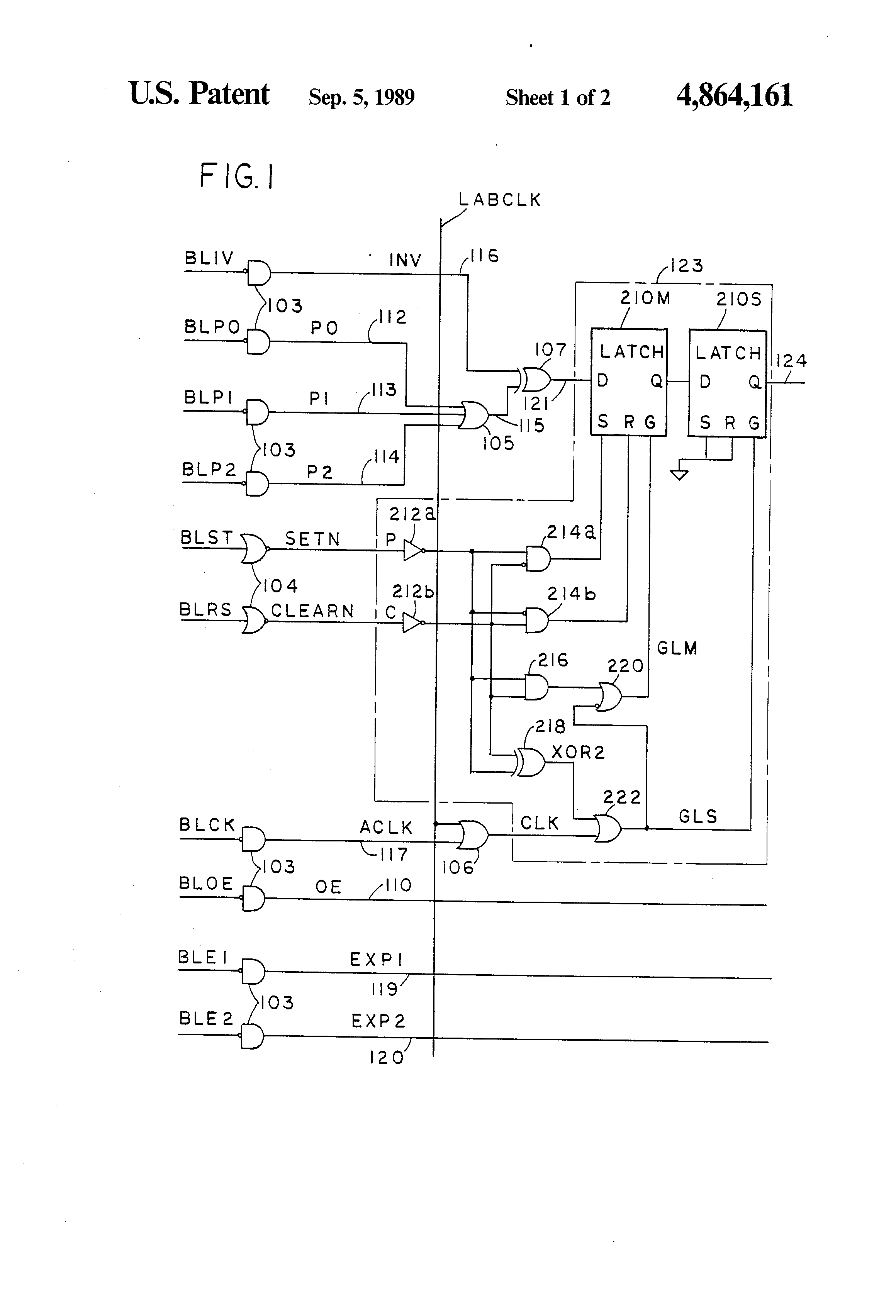
FIG. 1 is a schematic block diagram of an illustrative embodiment of the circuit of this invention.

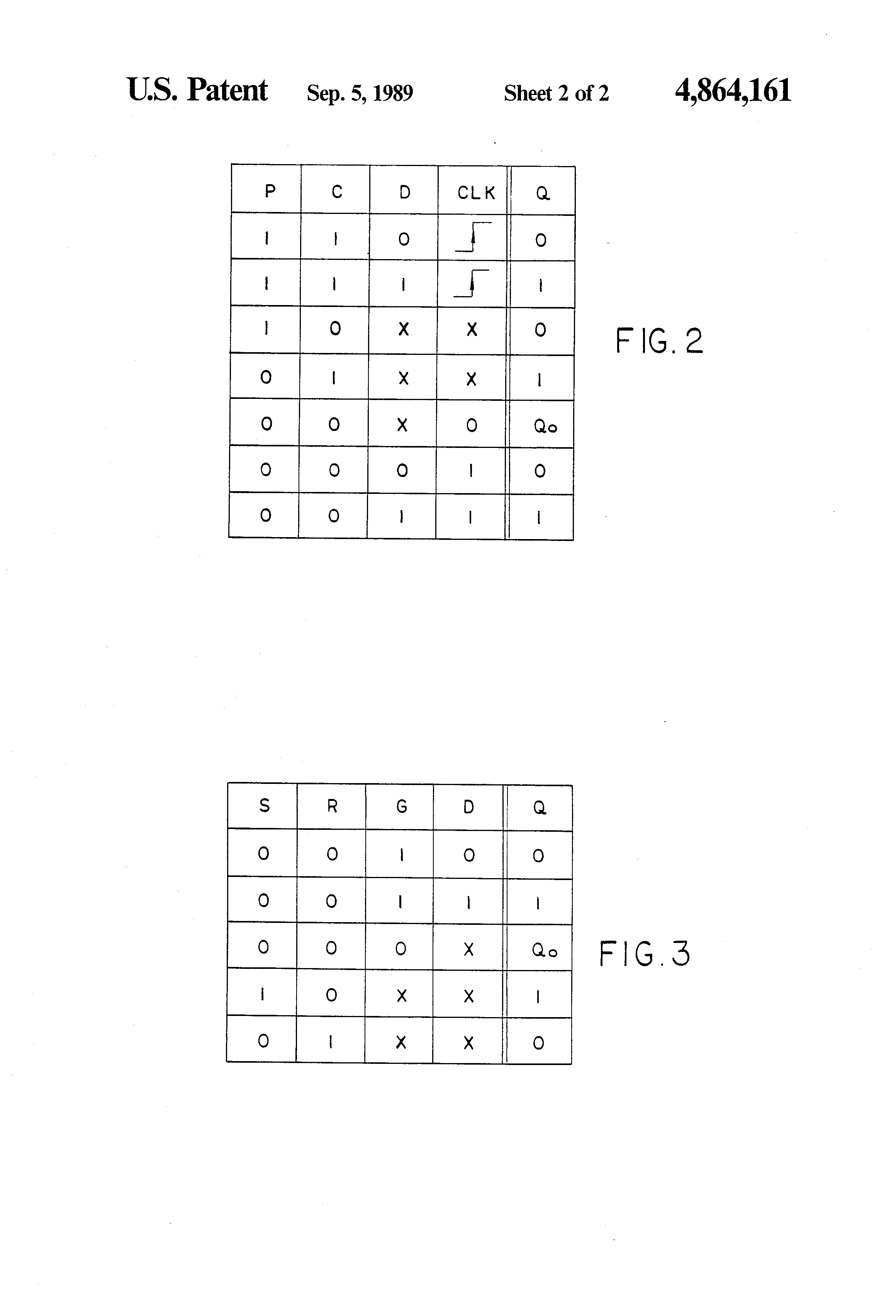
FIG. 2 is a truth table useful in explaining the operation of the circuit of FIG. 1.

FIG. 3 is a truth table useful in explaining the operation of two of the components of the circuit of FIG. 1.

DETAILED DESCRIPTION OF THE PREFERRED EMBODIMENTS

FIG. 1 shows part of the circuitry shown in FIG. 5 of application Ser. No. 190,663. (FIG. 1 is also similar to a portion of FIG. 4 in Ser. No. 190,571, but for convenience herein, only FIG. 5 of Ser. No. 190,663 is referred to below.) Similar names and reference numbers are used for similar elements in these two drawings, although the pictorial arrangement of the elements differs sightly from one drawing to the other. The elements surrounded by chain-dotted line 123 herein correspond to flip-flop 123 in Ser. No. 190,663. (Inverters 212 correspond to the active-low inputs shown on the P and C terminals of flip-flop 123 in that application.)

FIG. 2 is a truth table for the overall operation of flip-flop 123. (FIG. 2 corresponds to FIG. 9 in Ser. No. 190,663 and to FIG. 8 in Ser. No. 190,571.) The first four lines of FIG. 2 show that when one or both of the preset P and clear C signals is 1, flip-flop 123 operates like a normal D flip-flop. The last three lines of FIG. 2 show that when P and C are both O (which is normally an illegal condition for a D flip-flop with active-low inputs), flip-flop 123 acts like a flow-through devicce (i.e., Q=D, assuming that the clock signal CLK remains high as shown in the last two lines of FIG. 2), but that (as shown in the third from the last line in FIG. 9) the flow-through data can also be latched into flip-flop 123 by causing CLK to go low (because Qo indicates that Q then holds whatever value it had just before CLK went low). In other words, in addition to being capable of operating as a D flip-flop (first four lines of FIG. 2) or as a flow-through device (last two lines of FIG. 2), flip-flop 123 can also act as a level-sensitive latch by latching in the flow-through data when CLK goes low (third from last line of FIG. 2). FIG. 1 shows the detailed construction of device 123 in accordance with the principles of this invention in order to realize the above-described modes of operation.

Each of latches 210M and 210S is a conventional D latch. Latch 210M is the so-called "master" latch, while latch 210S is the so-called "slave" latch. Each of latches 210 has a data input terminal D, an output terminal Q, a set input terminal S, a reset input terminal R, and a gate or "function enable" input terminal G. FIG. 3 is a truth table for the operation of each of latches 210. As shown in that FIG., when both the set S and reset R inputs of a latch 210 are O and the gate G input is 1, then the Q output follows the data D input. However, when all of S, R, and G are O, the Q output holds whatever value (denoted Qo) it had just before G went low. In other words, with S and R both O, Q is insensitive to changes in D while G is low. When S is 1 and R is O, Q is 1 regardless of G and D. Similarly, when S is O and R is 1, Q is O regardless of G and D. In the ensuing discussion, an M or S suffix is sometimes used to distinguish the signals associated with master latch 210M from the signals associated with slave latch 210S. For example, DM refers to the D signal of master latch 210M, while DS refers to the D signal of slave latch 210S.

The P and C signals (corresponding respectively to the P and C signals in Ser. No. 190,663 ) and to the PRE and CLR signals in Ser. No. 190,571) are respectively inverted by inverters 212a and 212b and then applied to one input of each of AND gates 214a and 214b. The inverse of the inverted C signal is applied to the other input of AND gate 214a, and the inverse of the inverted P signal is applied to the other input of AND gate 214b. The effect of AND gates 214 is to make it impossible for both SM and RM to be 1 at the same time. Assuming, however, that no more than one of P and C is 0, gates 214 effectively apply the inverted P signal to the S terminal of latch 210M, and the inverted C signal to the R terminal of latch 210M. Accordingly, if either P or C is 0 QM is determined by which of P and C is 0. QM is then passed through to QS because with either P or C 0, the output XOR2 of EXCLUSIVE OR ("XOR") gate 218 becomes 1 and the output GLS of OR gate 222 also becomes 1. (SS and RS are always tied low.) The above-described operation corresponds to the third and fourth lines of FIG. 2.

If both P and C are 1, SM and RM are both O. The output of AND gate 216 is O, and so is the output of XOR gate 218. OR gate 222 then passes whatever CLK signal is applied to it, and that signal is inverted by OR gate 220. Assuming that the CLK signal is initially low, GM is high and DM is passed to QM and thereby applied to DS. When the CLK signal subsequently goes high, DS is passed to QS. This mode of operation corresponds to the first two lines of FIG. 2.

If P and C are both 0, SM and SR are also both O. The output of AND gate 216 is 1, the output of OR gate 220 is 1, and the output of XOR gate 218 is O. If CLK is also 1 (e.g., because BLCK is tied low), the output of OR gate 106 is 1, and the output of OR gate 222 is also 1. This means that each of latches 210 operates as shown in the first two lines of FIG. 3 so that QS=DM. In other words, whatever data is applied to DM flows through to QS. This mode of operation corresponds to the last two lines of FIG. 2.

If, at any time during the flow-through operation described immediately above, CLK goes low (e.g., because BLCK is not in fact permanently tied low), the output of OR gate 222 becomes O. This causes latch 210S to operate as shown in the third line in FIG. 3, thereby latching in the current value Qo of QS. This mode of operation corresponds to the fifth line of FIG. 2.

From the foregoing, it will be apparent that the circuit of FIG. 3 can be used to supply on lead 124 either the "registered" or "combinatorial" output of XOR gate 107 (registered output results from operation of device 123 as a D flip-flop (first four lines of FIG. 2); combinatorial output results from operation of device 123 in the flow-through mode (last two lines of FIG. 2)), and that in addition, the flow-through mode data can be latched into device 123 at any time by causing the CLK signal to go low. Device 123 is therefore highly flexible and of great utility in programmable logic device ("PLDs") such as are shown in Ser. Nos. 190,663 and 190,571.

Although particular signal values like "0" and "1" or "first polarity" and "second polarity" are referred to herein and in the appended claims, it will be understood that these values and terms are purely arbitrary, and that they are used solely for purposes of illustration. Thus, for example, although "first polarity" is uniformly equated with logic 0, and "second polarity" is uniformly equated with logic 1 herein as an aid to understanding the specification and claims, this is not necessarily the case, and the polarity or value of various signals can be reversed or otherwise altered without departing from the scope and spirit of the invention. As another example, whereas the specification and claims sometimes refer to applying the inverse of a particular signal to a particular component, if the polarity of that signal were reversed, then the signal could be applied directly (without inversion) to that component. Again, such polarity reversals and the consequent elimination (or addition) of inversions is entirely within the scope of the invention.
Claims (8)

  1. A multifunctional flip-flop-type device having data, preset, clear, and clock input terminals, and a data output terminal comprising: first means for applying the signal applied to the data input terminal to the data output terminal when the preset and clear signals have a second polarity and the clock signal changes from a first polarity to a second polarity; second means for applying a signal having a first polarity to the data output terminal when the preset signal has a second polarity and the clear signal has a first polarity, and for applying a signal having a second polarity to the data output terminal when the preset signal has a first polarity and the clear signal has a second polarity; third means for holding the signal applied to the data output terminal constant when the preset, clear, and clock signals have a first polarity; and fourth means for applying the signal applied to the data input terminal to the data output terminal when the preset and clear signals have a first polarity and the clock signal has a second polarity.
  2. A multimodal flip-flop-type device comprising: first and second D latches, each having a data input terminal, a set input terminal, a reset input terminal, a gate input terminal, and a data output terminal, the data output terminal of the first latch being connected to the data input terminal of the second latch, and the set and reset terminals of the second latch being connected to a source of a signal having a first polarity; a preset signal source; a clear signal source; a clock signal source; first means responsive to said preset and clear signals for applying the inverse of said preset signal to the set input terminal of said first latch and for applying the inverse of said clear signal to the reset terminal of said first latch unless both of said preset and clear signals have a first polarity, in which case said first means applies a signal having a first polarity to said set and reset terminals of said first latch; second means responsive to said preset and clear signals for applying a signal having a second polarity to the gate input terminal of said first latch when both of said preset and clear signals have said first polarity; third means responsive to said preset and clear signals for applying a signal having a second polarity to the gate input terminal of said second latch when either but not both of said preset and clear signals have said first polarity; and fourth means responsive to said preset, clear, and clock signals for applying the inverse of said clock signal to the gate input terminal of said first latch unless at least one of said preset and clear signals has said first polarity, and for applying said clock signal to the gate input terminal of said second latch unless one but not both of said preset and clear signals has said first polarity.
  3. The apparatus defined in claim 2 wherein said first means comprises: a first AND gate having the inverse of the preset signal connected to one of its inputs and the clear signal applied to the other of its inputs, and having its output signal applied to the set input terminal of said first latch; and a second AND gate having the inverse of the clear signal applied to one of its inputs and the preset signal applied to the other of its inputs, and having its output signal applied to the reset input terminal of said first latch.
  4. the apparatus defined in claim 2 wherein said second means comprises: a third AND gate having the inverse of the preset signal applied to one of its inputs and the inverse of the clear signal applied to the other of its inputs; and means for selectively applying the output signal of said third AND gate to the gate input terminal of said first latch.
  5. The apparatus defined in claim 2 wherein said third means comprises: an EXCLUSIVE OR gate having the inverse of the preset signal applied to one of its inputs and the inverse of the clear signal applied to the other of its inputs; and means for selectively applying the output signal of said EXCLUSIVE OR gate to the gate input terminal of said second latch.
  6. The apparatus defined in claim 5 wherein said means for selectively applying the output signal of said EXCLUSIVE OR gate to the gate input terminal of said second latch comprises: a first OR gate having the output signal of said EXCLUSIVE OR gate applied to one of its inputs and said clock signal applied to the other of its inputs, and having its output signal applied to the gate input terminal of said second latch.
  7. The apparatus defined in claim 6 wherein said second means comprises: a third AND gate having the inverse of the preset signal applied to one of its inputs and the inverse of the clear signal applied to the other of its inputs; and a second OR gate having the output signal of said second AND gate applied to one of its inputs and the inverse of the output signal of said first OR gate applied to the other of its inputs, and having its output signal applied to the gate input terminal of said first latch.
  8. The apparatus defined in claim 2 wherein said fourth means comprises: a third AND gate having the inverse of the preset signal applied to one of its inputs and the inverse of the clear signal applied to the other of its inputs; an EXCLUSIVE OR gate having the inverse of the preset signal applied to one of its inputs and the inverse of the clear signal applied to the other of its inputs; a first OR gate having the output of said EXCLUSIVE OR gate applied to one of its inputs and the clock signal applied to the other of its inputs, and having its output signal applied to the gate input terminal of said second latch; and a second OR gate having the output of said third AND gate applied to one of its inputs and the inverse of the output signal of said first OR gate applied to the other of its inputs, and having its output signal applied to the gate input terminal of said first latch.

Publications

Related applications (6)

  1. US07/190,530

    Priority application

  2. EP89301782A

    Priority application

  3. DE68915348T

    Priority application

  4. JP1112330A

    Priority application

  5. US07/190,530

    Claims priority

  6. US07/190,530

    Patent family

Record timeline

  1. Application filed by Altera Corp

  2. Priority to US07/190,530

  3. Assigned to ALTERA CORPORATION

  4. Priority to EP89301782A

  5. Priority to DE68915348T

  6. Priority to JP1112330A

  7. Application granted

  8. Publication of US4864161A

  9. Assigned to ALTERA CORPORATION (A CORPORATION OF DELAWARE)

  10. Assigned to ALTERA CORPORATION, A DELAWARE CORPORATION

  11. Anticipated expiration

  12. Expired - LifetimeCurrent

Legal events

  1. AS

    Assignment

    Owner name: ALTERA CORPORATION, 3525 MONROE STREET, SANTA CLAR

    Free format text: ASSIGNMENT OF ASSIGNORS INTEREST.;ASSIGNORS:NORMAN, KEVIN A.;SO, HOCK-CHUEN;VEENSTRA, KERRY S.;AND OTHERS;REEL/FRAME:004893/0587

    Effective date: 19880504

    Owner name: ALTERA CORPORATION, CALIFORNIA

    Free format text: ASSIGNMENT OF ASSIGNORS INTEREST;ASSIGNORS:NORMAN, KEVIN A.;SO, HOCK-CHUEN;VEENSTRA, KERRY S.;AND OTHERS;REEL/FRAME:004893/0587

    Effective date: 19880504

  2. STCF

    Information on status: patent grant

    Free format text: PATENTED CASE

  3. FEPP

    Fee payment procedure

    Free format text: PAYOR NUMBER ASSIGNED (ORIGINAL EVENT CODE: ASPN); ENTITY STATUS OF PATENT OWNER: LARGE ENTITY

  4. FPAY

    Fee payment

    Year of fee payment: 4

  5. FP

    Lapsed due to failure to pay maintenance fee

    Effective date: 19930905

  6. FEPP

    Fee payment procedure

    Free format text: PAYOR NUMBER ASSIGNED (ORIGINAL EVENT CODE: ASPN); ENTITY STATUS OF PATENT OWNER: LARGE ENTITY

    Free format text: PAYER NUMBER DE-ASSIGNED (ORIGINAL EVENT CODE: RMPN); ENTITY STATUS OF PATENT OWNER: LARGE ENTITY

  7. FPAY

    Fee payment

    Year of fee payment: 8

  8. AS

    Assignment

    Owner name: ALTERA CORPORATION (A CORPORATION OF DELAWARE), CA

    Free format text: MERGER;ASSIGNOR:ALTERA CORPORATION (A CORPORATION OF CALIFORNIA);REEL/FRAME:008811/0577

    Effective date: 19970618

  9. AS

    Assignment

    Owner name: ALTERA CORPORATION, A DELAWARE CORPORATION, CALIFO

    Free format text: MERGER;ASSIGNOR:ALTERA CORPORATION, A CALIFORNIA CORPORATION;REEL/FRAME:009015/0336

    Effective date: 19970325

  10. FPAY

    Fee payment

    Year of fee payment: 12

Patent citations (17)

  1. US3566153A

    Programmable sequential logic

    Texas Instruments Inc · February 23, 1971 · Examiner cited

  2. US4124899A

    Programmable array logic circuit

    Monolithic Memories, Inc. · November 7, 1978 · Examiner cited

  3. US4124899B1

    April 28, 1987 · Examiner cited

  4. US4422072A

    Field programmable logic array circuit

    Signetics Corporation · December 20, 1983 · Examiner cited

  5. US4717912A

    Apparatus for producing any one of a plurality of signals at a single output

    Advanced Micro Devices, Inc. · January 5, 1988 · Examiner cited

  6. US4791602A

    Soft programmable logic array

    Control Data Corporation · December 13, 1988 · Examiner cited

  7. US4617479A

    Programmable logic array device using EPROM technology

    Altera Corporation · October 14, 1986 · Examiner cited

  8. US4617479B1

    Programmable logic array device using eprom technology

    Altera Semiconductor Corp. · September 21, 1993 · Examiner cited

  9. US4689497A

    Master-slave type flip-flop circuits

    Nec Corporation · August 25, 1987 · Examiner cited

  10. US4609986A

    Programmable logic array device using EPROM technology

    Altera Corporation · September 2, 1986 · Examiner cited

  11. US4692633A

    Edge sensitive single clock latch apparatus with a skew compensated scan function

    International Business Machines Corporation · September 8, 1987 · Examiner cited

  12. US4677318A

    Programmable logic storage element for programmable logic devices

    Altera Corporation · June 30, 1987 · Examiner cited

  13. US4713792A

    Programmable macrocell using eprom or eeprom transistors for architecture control in programmable logic circuits

    Altera Corporation · December 15, 1987 · Examiner cited

  14. US4771285A

    Programmable logic cell with flexible clocking and flexible feedback

    Advanced Micro Devices, Inc. · September 13, 1988 · Examiner cited

  15. US4703206A

    Field-programmable logic device with programmable foldback to control number of logic levels

    Signetics Corporation · October 27, 1987 · Examiner cited

  16. US4756006A

    Bus transceiver

    International Business Machines Corporation · July 5, 1988 · Examiner cited

  17. US4758747A

    Programmable logic device with buried registers selectively multiplexed with output registers to ports, and preload circuitry therefor

    Advanced Micro Devices, Inc. · July 19, 1988 · Examiner cited

Non-patent citations (8)

  1. E. Goetting et al., "A CMOS Electrically-Reprogrammable ASIC with Multi-Level Random Logic Capabilities", 1986 IEEE International Solid-State Circuits Conference, pp. 244-245 and 359-360, 1986.
  2. E. Goetting et al., A CMOS Electrically Reprogrammable ASIC with Multi Level Random Logic Capabilities , 1986 IEEE International Solid State Circuits Conference, pp. 244 245 and 359 360, 1986.
  3. Farrell et al., "Edge-Triggered LSSD Compatible Set/Reset Latch", IBM T.D.B., vol. 26, No. 5, Oct. 1983, pp. 2249-2250, (307/272.2).
  4. Farrell et al., Edge Triggered LSSD Compatible Set/Reset Latch , IBM T.D.B., vol. 26, No. 5, Oct. 1983, pp. 2249 2250, (307/272.2).
  5. Puri et al., "Flush-Through Latch", IBM T.D.B., vol. 24, No. 7A, Dec. 1981, pp. 3115-3116, (307/480).
  6. Puri et al., Flush Through Latch , IBM T.D.B., vol. 24, No. 7A, Dec. 1981, pp. 3115 3116, (307/480).
  7. R. R. Munoz et al., "Automatic Partitioning of Programmable Logic Devices," VLSI Systems Design, Oct. 1987, pp. 74-76, 78, and 86.
  8. R. R. Munoz et al., Automatic Partitioning of Programmable Logic Devices, VLSI Systems Design, Oct. 1987, pp. 74 76, 78, and 86.

Cited by (102)

  1. US5072132A

    Vsli latch system and sliver pulse generator with high correlation factor

    Digital Equipment Corporation · December 10, 1991 · Examiner cited

  2. JP2579237B2

    State element circuit having a flow-through latch circuit, VLSI circuit having the state element circuit, and method of operating a latch as a functional alternative to a master-slave flip-flop

    ディジタル イクイプメント コーポレーション · February 5, 1997

  3. US5003204A

    Edge triggered D-type flip-flop scan latch cell with recirculation capability

    Bull Hn Information Systems Inc. · March 26, 1991 · Examiner cited

  4. US5220214A

    Registered logic macrocell with product term allocation and adjacent product term stealing

    Altera Corporation · June 15, 1993 · Examiner cited

  5. US6707315B2

    Registered logic macrocell with product term allocation and adjacent product term stealing

    Altera Corporation · March 16, 2004

  6. US6157208A

    Programmable logic device macrocell with improved logic capability

    Altera Corporation · December 5, 2000 · Examiner cited

  7. US5598108A

    High-density erasable programmable logic device architecture using multiplexer interconnections, and registered macrocell with product term allocation and adjacent product term stealing

    Altera Corporation · January 28, 1997 · Examiner cited

  8. US6366119B1

    Programmable logic device macrocell with improved logic capability

    Altera Corporation · April 2, 2002

  9. US5861760A

    Programmable logic device macrocell with improved capability

    Altera Corporation · January 19, 1999 · Examiner cited

  10. US5357144A

    Complementary logic circuit

    Sony Corporation · October 18, 1994 · Examiner cited

  11. US5350954A

    Macrocell with flexible product term allocation

    Altera Corporation · September 27, 1994 · Examiner cited

  12. US5384494A

    Programmable hold-off for integrated circuit I/O pins

    Hughes Aircraft Company · January 24, 1995 · Examiner cited

  13. US5416362A

    Transparent flip-flop

    Unisys Corporation · May 16, 1995 · Examiner cited

  14. US5638018A

    P-type flip-flop

    Advanced Micro Devices, Inc. · June 10, 1997 · Examiner cited

  15. US5719516A

    Lock generator circuit for use with a dual edge register that provides a separate enable for each use of an input clock signal

    Advanced Micro Devices, Inc. · February 17, 1998 · Examiner cited

  16. US6294928B1

    Programmable logic device with highly routable interconnect

    Altera Corporation · September 25, 2001

  17. US6414514B1

    Logic device architecture and method of operation

    Altera Corporation · July 2, 2002

  18. US6492834B1

    Programmable logic device with highly routable interconnect

    Altera Corporation · December 10, 2002

  19. US6265922B1

    Controllable latch/register circuit

    Lsi Logic Corporation · July 24, 2001

  20. GB2332792B

    Controllable latch/register circuit

    Lsi Logic Corp · June 21, 2000 · Examiner cited

  21. GB2332792A

    Controllable latch/register circuit

    Lsi Logic Corp · June 30, 1999 · Examiner cited

  22. US6629276B1

    Method and apparatus for a scannable hybrid flip flop

    Bae Systems Information And Electronic Systems Integration, Inc. · September 30, 2003

  23. US20060152248A1

    Configuration circuits for programmable logic devices

    Madurawe Raminda U · July 13, 2006 · Examiner cited

  24. US20070210830A1

    Three dimensional integrated circuits

    Madurawe Raminda U · September 13, 2007 · Examiner cited

  25. US10339245B2

    Timing exact design conversions from FPGA to ASIC

    Callahan Cellular L.L.C. · July 2, 2019

  26. US9912336B2

    Three dimensional integrated circuits

    Callahan Cellular L.L.C. · March 6, 2018

  27. US10447272B2

    Three dimensional integrated-circuits

    Callahan Cellular L.L.C. · October 15, 2019

  28. US20060150137A1

    Three dimensional integrated circuits

    Madurawe Raminda U · July 6, 2006 · Examiner cited

  29. US7538575B2

    Three dimensional integrated circuits

    Tier Logic, Inc. · May 26, 2009

  30. US20060158217A1

    Timing exact design conversions from FPGA to ASIC

    Madurawe Raminda U · July 20, 2006 · Examiner cited

  31. US7627848B2

    Bit stream compatible FPGA to MPGA conversions

    Tier Logic, Inc. · December 1, 2009

  32. US9547736B2

    Timing exact design conversions from FPGA to ASIC

    Callahan Cellular L.L.C. · January 17, 2017

  33. US20070103192A1

    Bit stream compatible FPGA to MPGA design conversions

    Madurawe Raminda U · May 10, 2007 · Examiner cited

  34. US20070152708A1

    MPGA products based on a prototype FPGA

    Madurawe Raminda U · July 5, 2007 · Examiner cited

  35. US9240790B2

    Three dimensional integrated circuits

    Callahan Cellular L.L.C. · January 19, 2016

  36. US7673273B2

    MPGA products based on a prototype FPGA

    Tier Logic, Inc. · March 2, 2010

  37. US7268580B2

    Configuration circuits for three dimensional programmable logic devices

    Viciciv Technology · September 11, 2007

  38. US8856699B2

    Three dimensional integrated circuits

    Raminda Udaya Madurawe · October 7, 2014

  39. US20070210336A1

    Semiconductor devices fabricated with different processing options

    Madurawe Raminda U · September 13, 2007 · Examiner cited

  40. US20050102646A1

    Configuration circuits for three dimensional programmable logic devices

    Madurawe Raminda U. · May 12, 2005 · Examiner cited

  41. US7285982B2

    Configuration circuits for programmable logic devices

    Viciciv Technology · October 23, 2007

  42. US8829664B2

    Three dimensional integrated circuits

    Raminda Udaya Madurawe · September 9, 2014

  43. US8499269B2

    Timing exact design conversions from FPGA to ASIC

    Raminda Udaya Madurawe · July 30, 2013

  44. US20080067594A1

    Insulated-gate field-effect thin film transistors

    Madurawe Raminda U · March 20, 2008 · Examiner cited

  45. US20080074146A1

    Three dimensional integrated circuits

    Madurawe Raminda U · March 27, 2008 · Examiner cited

  46. US7356799B2

    Timing exact design conversions from FPGA to ASIC

    Viciciv Technology, Inc. · April 8, 2008

  47. US7362133B2

    Three dimensional integrated circuits

    Viciciv Technology, Inc. · April 22, 2008

  48. US8429585B2

    Three dimensional integrated circuits

    Raminda Udaya Madurawe · April 23, 2013

  49. US20080191738A1

    Three dimensional integrated circuits

    Raminda Udaya Madurawe · August 14, 2008 · Examiner cited

  50. US20080218205A1

    Timing Exact Design Conversions from FPGA to ASIC

    Raminda Udaya Madurawe · September 11, 2008 · Examiner cited

  51. US7446563B2

    Three dimensional integrated circuits

    Tier Logic · November 4, 2008

  52. US20090004788A1

    Thin film transistors and fabrication methods

    Raminda Udaya Madurawe · January 1, 2009 · Examiner cited

  53. US20110102014A1

    Three dimensional integrated circuits

    Raminda Udaya Madurawe · May 5, 2011 · Examiner cited

  54. US7759705B2

    Semiconductor devices fabricated with different processing options

    Tier Logic, Inc. · July 20, 2010

  55. US9070668B2

    Pads and pin-outs in three dimensional integrated circuits

    Yakimishu Co. Ltd. L.L.C. · June 30, 2015

  56. US9679914B2

    Pads and pin-outs in three dimensional integrated circuits

    Callahan Cellular L.L.C. · June 13, 2017

  57. US20060146596A1

    Configurable storage device

    Madurawe Raminda U · July 6, 2006 · Examiner cited

  58. US7298641B2

    Configurable storage device

    Viciciv Technology · November 20, 2007

  59. US20040080999A1

    Configurable storage device

    Madurawe Raminda Udaya · April 29, 2004 · Examiner cited

  60. US7042756B2

    Configurable storage device

    Viciciv Technology · May 9, 2006

  61. US7679399B2

    Programmable interconnect structures

    Tier Logic, Inc. · March 16, 2010

  62. US20090039917A1

    Programmable Interconnect Structures

    Raminda Udaya Madurawe · February 12, 2009 · Examiner cited

  63. US7088136B1

    Programmable logic device latch circuits

    Altera Corporation · August 8, 2006

  64. US9882567B2

    Programmable structured arrays

    Callahan Cellular L.L.C. · January 30, 2018

  65. US8810276B2

    Programmable structured arrays

    Raminda U. Madurawe · August 19, 2014

  66. US20060181308A1

    Programmable structured arrays

    Raminda Udaya Madurawe · August 17, 2006 · Examiner cited

  67. US9397665B2

    Programmable structured arrays

    Callahan Cellular L.L.C. · July 19, 2016

  68. US7323905B2

    Programmable structured arrays

    Viciciv Technology · January 29, 2008

  69. US8274309B2

    Programmable structured arrays

    Raminda Udaya Madurawe · September 25, 2012

  70. US20090134909A1

    Programmable structured arrays

    Raminda Udaya Madurawe · May 28, 2009 · Examiner cited

  71. US10594320B2

    Programmable structured arrays

    Callahan Cellular L.L.C. · March 17, 2020

  72. US20070152707A1

    Integrated circuits with RAM and ROM fabrication options

    Madurawe Raminda U · July 5, 2007 · Examiner cited

  73. US7265577B2

    Integrated circuits with RAM and ROM fabrication options

    Viciciv Technology · September 4, 2007

  74. US20050180044A1

    Damping structure of a hard disk drive

    Samsung Electronics Co., Ltd. · August 18, 2005 · Examiner cited

  75. US7489164B2

    Multi-port memory devices

    Raminda Udaya Madurawe · February 10, 2009

  76. US20080106953A1

    Multi-port memory devices

    Madurawe Raminda U · May 8, 2008 · Examiner cited

  77. US8397067B1

    Mechanisms and techniques for protecting intellectual property

    Altera Corporation · March 12, 2013

  78. US8670561B1

    Method and apparatus for limiting use of IP

    Altera Corporation · March 11, 2014

  79. US20070210826A1

    Programmable logic devices comprising time multiplexed programmable interconnect

    Madurawe Raminda U · September 13, 2007 · Examiner cited

  80. US7486111B2

    Programmable logic devices comprising time multiplexed programmable interconnect

    Tier Logic, Inc. · February 3, 2009

  81. USRE45110E1

    MPGA products based on a prototype FPGA

    Raminda Udaya Madurawe · September 2, 2014

  82. US20090128188A1

    Pad invariant FPGA and ASIC devices

    Raminda Udaya Madurawe · May 21, 2009 · Examiner cited

  83. US9978773B2

    Pads and pin-outs in three dimensional integrated circuits

    Callahan Cellular L.L.C. · May 22, 2018

  84. US8643162B2

    Pads and pin-outs in three dimensional integrated circuits

    Raminda Udaya Madurawe · February 4, 2014

  85. US20090129174A1

    Multi-port thin-film memory devices

    Raminda Madurawe · May 21, 2009 · Examiner cited

  86. US20090146189A1

    Pads and pin-outs in three dimensional integrated circuits

    Raminda Udaya Madurawe · June 11, 2009 · Examiner cited

  87. US7812458B2

    Pad invariant FPGA and ASIC devices

    Tier Logic, Inc. · October 12, 2010

  88. US10304854B2

    Pads and pin-outs in three dimensional integrated circuits

    Callahan Cellular L.L.C. · May 28, 2019

  89. US7635988B2

    Multi-port thin-film memory devices

    Tier Logic, Inc. · December 22, 2009

  90. US20090128189A1

    Three dimensional programmable devices

    Raminda Udaya Madurawe · May 21, 2009 · Examiner cited

  91. US7795913B2

    Programmable latch based multiplier

    Tier Logic · September 14, 2010

  92. US7602213B2

    Using programmable latch to implement logic

    Tier Logic, Inc. · October 13, 2009

  93. US7573294B2

    Programmable logic based latches and shift registers

    Tier Logic, Inc. · August 11, 2009

  94. US7573293B2

    Programmable logic based latches and shift registers

    Tier Logic, Inc. · August 11, 2009

  95. US20090167349A1

    Programmable logic based latches and shift registers

    Raminda Madurawe · July 2, 2009 · Examiner cited

  96. US20090167348A1

    Programmable latch based multiplier

    Nij Dorairaj · July 2, 2009 · Examiner cited

  97. US20090167350A1

    Programmable logic based latches and shift registers

    Raminda Madurawe · July 2, 2009 · Examiner cited

  98. US20090167347A1

    Using programmable latch to implement logic

    Nij Dorairaj · July 2, 2009 · Examiner cited

  99. US9087169B2

    Automated metal pattern generation for integrated circuits

    Raminda U. Madurawe · July 21, 2015

  100. US8159268B1

    Interconnect structures for metal configurable integrated circuits

    Raminda Udaya Madurawe · April 17, 2012

  101. US8159265B1

    Memory for metal configurable integrated circuits

    Raminda Udaya Madurawe · April 17, 2012

  102. US8159266B1

    Metal configurable integrated circuits

    Raminda Udaya Madurawe · April 17, 2012

Related Patents