Skip to content

Patent drawings

Drawing 1 of 2

US 4,899,070

Drawing 1 of 2

Expanded drawing 1 of 2 from US 4,899,070, Bit line sense amplifier for programmable logic devices
High-resolution patent drawing

US 4,899,070

Bit line sense amplifier for programmable logic devices

Filed
July 13, 1988
Granted
February 6, 1990
Assignee
Altera
Inventors
Jung-Hsing Ou, Sau-Ching Wong

Abstract

In a programmable logic device, switching speed is improved by preventing the bit line potential from going excessively close to ground even when large numbers of word line connections to the ground conductor are made. In addition, bit line pull up to logic 1 is effected more rapidly (without retarding bit line pull down to logic 0) by having two transistors connected in parallel with one another between the reference potential source and the bit line. One of these transistors is on all the time providing a relatively small leakage current. The other transistor is on only while the bit line is at logic 0, thereby speeding pull up to logic 1 and then shutting off so as not to impede subsequent return to logic 0.

View on Google Patents ↗
View Full PatentComplete archived record · 2 figures · 18 description paragraphs · 12 claims

Patent record

Source
Google Patents
Publication
US4899070A
Application
US07/218,556
Priority
July 13, 1988
Prior art date
July 13, 1988
Publication date
February 6, 1990
Legal status
Expired - Lifetime
Original assignee
Altera Corp
Current assignee
Altera Corp
Prior art keywords
electrical potential, bit line, line conductor, source, current
Source retrieved
July 20, 2026

Classifications

  • GPHYSICS
  • G11INFORMATION STORAGE
  • G11CSTATIC STORES
  • G11C16/00Erasable programmable read-only memories
  • G11C16/02Erasable programmable read-only memories electrically programmable
  • G11C16/06Auxiliary circuits, e.g. for writing into memory
  • G11C16/26Sensing or reading circuits; Data output circuits

Figures

2 plates

Figure 1 of 2 from US 4,899,070, Bit line sense amplifier for programmable logic devices
Figure 01Full resolution ↗
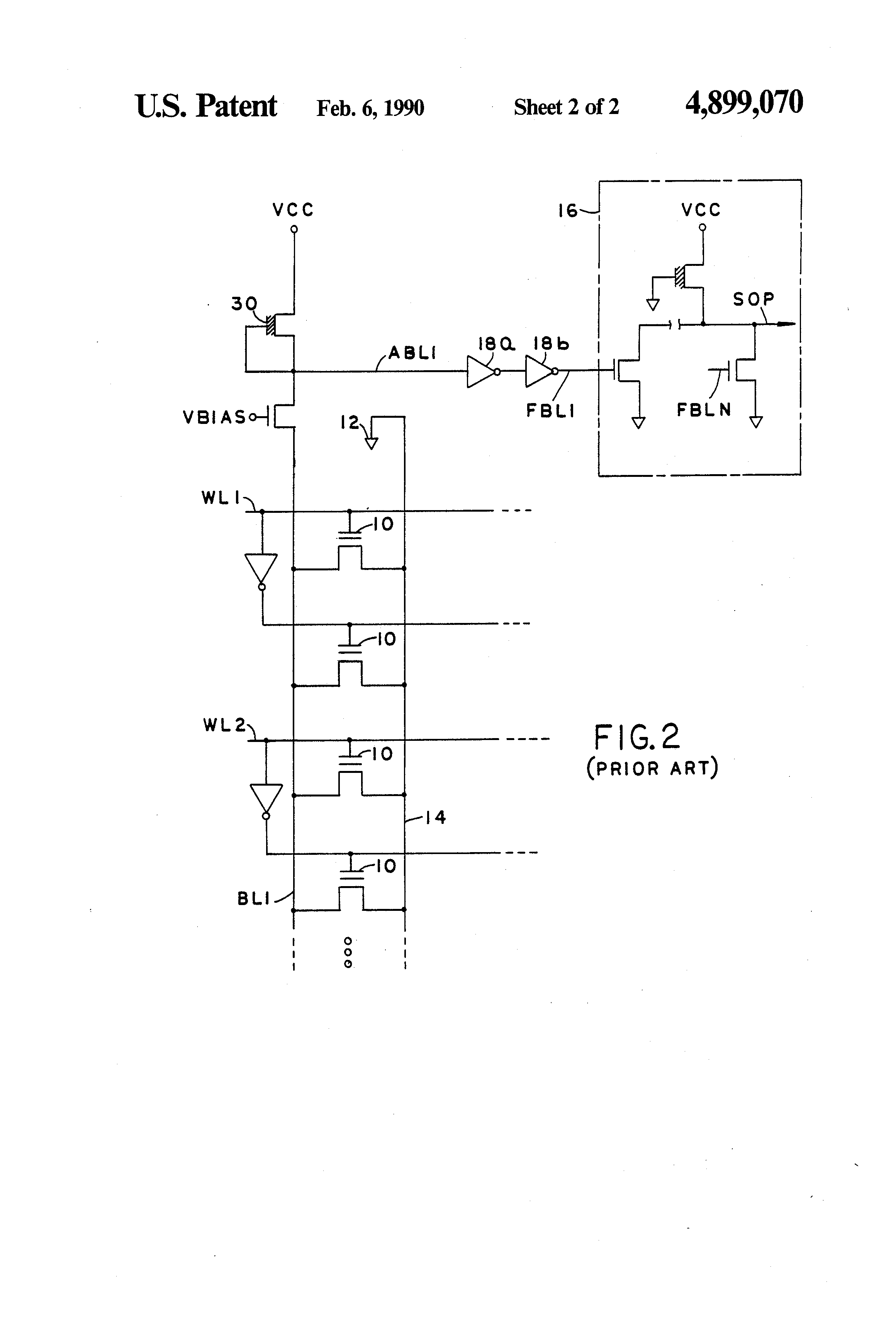
Figure 2 of 2 from US 4,899,070, Bit line sense amplifier for programmable logic devices
Figure 02Full resolution ↗

Description

BACKGROUND OF THE INVENTION

This invention relates to programmable logic devices ("PLDs"), and more particularly to improved bit line sense amplifiers for PLDs.

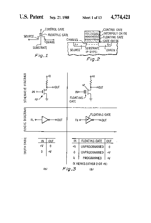
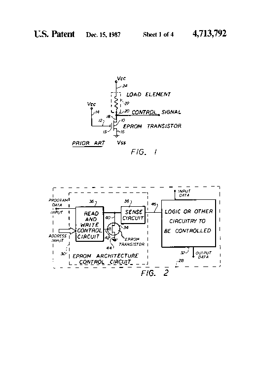
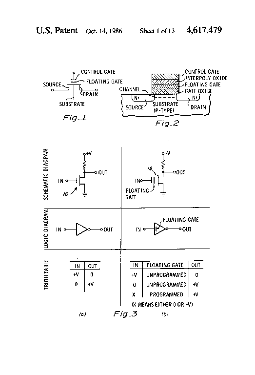
Programmable logic devices ("PLDs") are well known as shown, for example, by such references as Hartmann et al. U.S. Pat. Nos. 4,617,479; Hartmann et al. 4,609,986; Veenstra 4,677,318; Hartmann et al. 4,713,792; Birkner et al. 4,124,899; Cavlan 4,703,206; and Spencer 3,566,153, all of which are hereby incorporated by reference herein. There is a continuing demand for PLDs which are both larger and faster. However, these two objectives conflict with one another because as the number of interconnected devices increases (in order to provide larger PLDs capable of performing more complex logic functions), circuit loading and propagation delay also tend to increase, thereby tending to decrease the switching sped of the PLD.

In view of the foregoing it is an object of this invention to provide improved circuits for PLDs which increase the switching speed of the PLD (e.g., by counteracting the effects of increased circuit loading).

It is a more particular object of this invention to provide improved bit line sense amplifier circuits for PLDs (e.g., bit line sense amplifier circuits which are capable of faster switching speeds).

SUMMARY OF THE INVENTION

These and other objects of the invention are accomplished in accordance with the principles of the invention by providing a variable current limiting device (e.g., a transistor) in the circuit connecting each bit line array to ground. This variable current limiting device is controlled by a feedback signal from the bit line output so that when the bit line tends to go excessively low (e.g., because a large number of the electrically programmable read-only memory devices ("EPROMs") in that bit line array are turned on), the variable current limiting device becomes less conductive, thereby preventing the bit line output from going unnecessarily close to ground. Without the improvement of this invention, the bit line output signal could go very close to ground, thereby increasing the time required to pull it back up to logic 1 when all the associated EPROMs turn off.

Another feature of the invention also helps increase the speed at which the bit line output can be pulled up from logic 0 to logic 1. The pull-up function is performed by two pull-up transistors connected in parallel with one another between the source of relatively high reference potential (VCC) and the amplified bit line output. One of these pull-up transistors (which is preferably relatively small and which therefore provides only a relatively small "leakage" current) is controlled so that it is on at all times. The other pull-up transistor (which is preferably relatively large and therefore provides a relatively large current when it is on) is controlled so that it shuts off as soon as the bit line output switches to logic 1. Accordingly, this second pull-up transistor helps to rapidly pull up the bit line output during a transition from logic 0 to logic 1, but it does not subsequently slow down a transition from logic 1 to logic 0.

Further features of the invention, its nature and various advantages will be more apparent from the accompanying drawings and the following detailed description of the preferred embodiments.

BRIEF DESCRIPTION OF THE DRAWINGS

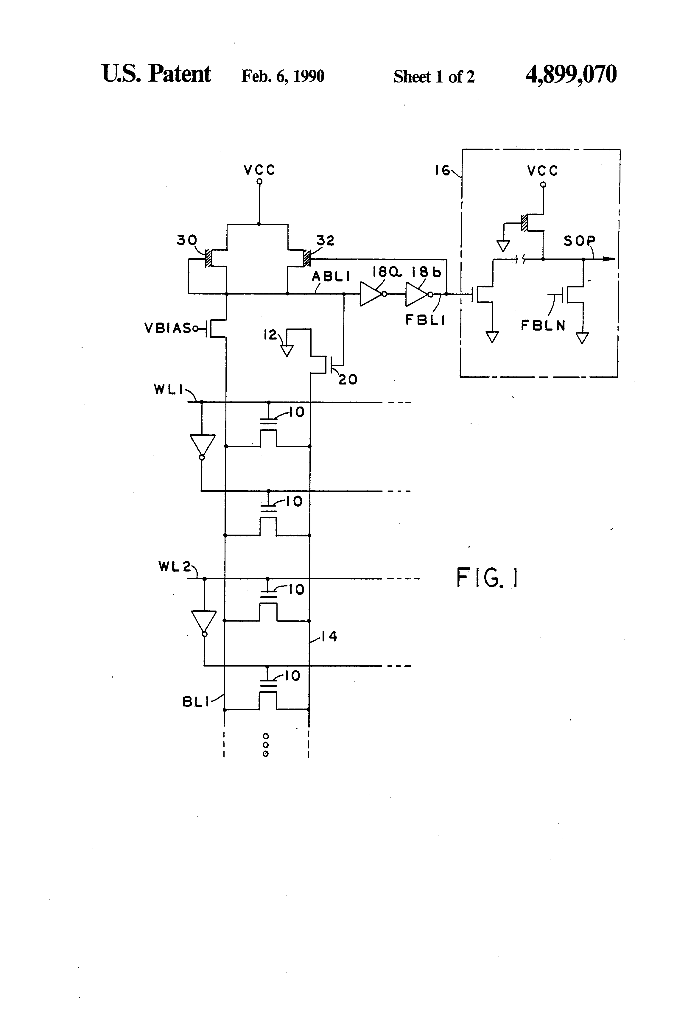
FIG. 1 is a schematic diagram of an illustrative embodiment of the invention.

FIG. 2 is a schematic diagram of a prior art circuit of the general type shown in FIG. 1, but without the features of the present invention.

DETAILED DESCRIPTION OF THE PREFERRED EMBODIMENTS

FIG. 1 shows part of the conventional circuitry for a PLD which has been modified in accordance with the principles of this invention. EPROMs 10 are programmable interconnections between each of a plurality of input word lines WL1, WL2, etc., and each of a plurality of bit lines BL1, BL2, etc. (only one of which is shown in FIG. 1). As is usual (although not always necessary), both the true and complement versions of each word line signal are connectable to each bit line.

EPROMs 10 are individually programmed in advance so that each EPROM either does or does not apply the associated work line signal (true or complement) to the associated bit line. For example if a particular EPROM 10 is programmed to apply associated (true or complement) word line signal to the associated, bit line, then when that (true or complement) word line signal is logic 1, the EPROM connects the bit line to "ground" (logic 0) at point 12 via the "virtual" ground line 14 and current limiting device 20 associated with that bit line. This causes the bit line to go low (logic 0), which in turn causes the amplified bit line signal (e.g., ABL1) and the final bit line signal (e.g., FBL1) to also go low. Typically (although not necessarily) several final bit line signals are combined in additional logic circuitry 16 to provide a sum-of-products output signal SOP which may be either output from the PLD or further processed in the PLD.

Typical voltages in the circuit are as follows: VCC is 5 volts; VBIAs is approximately 2.5 volts; ground (e.g., point 12) is 0 volts; logic 0 on BL1 is typically less than 1 volt; logic 1 on BL1 is typically greater than 1 volt; logic 0 on ABL1 is approximately 1.2 volts; logic 1 on ABL1 is 3 to 3.5 volts; logic 0 on FBL1 is approximately 0 volts; and logic 1 on FBL1 is approximately 5 volts. Thus inverters 18a and 18b collectively comprise a circuit for sensing the potential difference between the logical states of the ABL1 signal and for amplifying that signal to the normal CMOS (complementary metal oxide semiconductor) levels of 0 and 5 volts. It will be understood that the particular voltages mentioned above are merely illustrative, and that they are provided solely as an aid to understanding the depicted circuit. Those skilled in the art will appreciate that any or all of these voltages can be altered, even to the point of reversing polarities, without departing from the scope and spirit of the invention. For example, although "ground potential" is referred to herein and in the appended claims, it will be understood that this is merely an arbitrary term and that it is not used in any absolute sense. Thus the potential referred to as "ground potential" could be any potential different from (i.e., higher or lower than) VCC.

Although only a small number of word lines are shown connectable to bit line BL1 in FIG. 1, it is not at all unusual in current PLD designs for there to be 100 or more word lines connectable to each bit line. Similarly, although one one bit line BL1 is shown in FIG. 1, it is not at all unusual for there to be 100 or more bit lines connectable to each word line.

When only a relatively small number of the EPROMs connected to bit line BL1 are turned on, the voltage on BL1, although logic 0, may remain relatively high (e.g., typically less than but relatively close to 1 volt). Thereafter, when all of these EPROMs are turned off, the voltage on BL1 can be pulled up to logic 1 relatively quickly. However, when a relatively large number of the EPROMs connected to bit line BL1 are turned on in the absence of this invention (as in the case of the prior art circuit shown in FIG. 2), the voltage on BL1 tends to go very close to ground (e.g., very close to 0 volts). This means that it takes substantially longer to pull the voltage on BL1 up to logic 1 when all of the EPROMs turn off. This data pattern is normally the "worst case" for the transition of BL1 from logic 0 to logic 1.

In accordance with the present invention as shown in FIG. 1, current limiting transistor 20 is connected in series between the virtual ground line 14 associated with bit line BL1 and the actual source 12 of ground potential. (In the depicted embodiment, transistor 20 is an n-channel transistor which is off when its gate is low.) The gate of transistor 20 is connected to ABL1. Because the voltage of ABL1 is designed to be always higher than the threshold voltage of an n-channel transistor, transistor 20 is therefore on at all times. However, as the voltage on BL1 comes closer to ground and therefore the voltage on ABL1 also falls correspondingly, transistor 20 becomes less conducting. This prevents the voltage on BL1 from dropping excessively low even when large numbers of EPROMs 10 are conducting. THis in turn improves the switching speed of the device when all of EPROMs 10 turn off because the voltage on BL1 does not have to be pulled up so far to reach the threshold for logic 1.

Another aspect of the invention involves the provision of two transistors 30 and 32 connected in parallel with one another between reference potential source VCC and ABL1. (In the depicted embodiment, each of transistors 30 and 32 is a p-channel transistor which is off when its gate is high.) The gate of transistor 30 is connected to ABL1, while the gate of transistor 32 is connected to FBL1. Transistor 30 is preferably a relatively small device which is on at all times providing a relatively small "leakage" current from VCC to ABL1. Ideally, the logic 1 state of ABL1 should be biased close to the trip-point of the subsequent inverter stage 18a. In this embodiment, the logic 1 state of ABL1 is limited to VCC minus Vtp (where Vtp is the threshold voltage of p-channel transistor 30). Transistor 32, on the other hand, is preferably a relatively large device which is on only when ABL1 is logic 0. Thus when all of EPROMs 10 turn off, the relatively large current flowing through transistor 32 is available to help rapidly pull up ABL1 from logic 0 to logic 1. On the other hand, as soon as ABL1 reaches logic 1, transistor 32 shuts off so that it does not retard a subsequent transition from logic 1 to logic 0.

The difference in voltage on ABL1 between the logic states and the trip point of inverter state 18a determines the noise immunity of the sense amplifier stage. In this embodiment, inverter 18a is designed with its trip point at about one-half VCC or 2.5 volts. For logic 1, the noise margin is therefore calculated to be 0.5 VCC minus Vtp. For logic 0, ABL1's voltage is determined by the ratio of the combined currents through pull- up transistors 30 and 32 versus the current through the EPROM cell 10 and current limiting device 20. As mentioned above, the logic 0 state of ABL1 is about 1.2 volts. Therefore, the noise margin for logic 0 is calculated to be 0.5 VCC minus 1.2 volts. Because Vtp is typically about 1 volt, the noise margins for both logic states are similar.

It will be understood that the foregoing is merely illustrative of the principles of this invention, and that various modifications can be made by those skilled in the art without departing from the scope and spirit of the invention. For example, although particualr voltage values and device types (e.g., n-channel or p-channel transistors) have been mentioned, it will be understood that other voltages and devices can be used if desired. Thus transistor 30 could be an n-channel transistor with its gate tied to VCC. With this configuration, the logic state of ABL1 is limited to VCC minus Vtn (where Vtn is the threshold voltage of n-channel transistor 30).
Claims (12)

  1. A programmable logic device comprising: a bit line conductor; a source of ground electrical potential; a virtual ground line conductor; a plurality of word line conductors, each of which conducts an associated word line signal; a plurality of programmable interconnection devices, each of which, if programmed, is controlled by the word line signal on a respective one of said word line conductors to selectively connect said bit line conductor to said virtual ground line conductor; and variable current limiting means connected in series between said virtual ground line conductor and said source of ground electrical potential, said variable current limiting means being means responsive to the voltage of the signal on said bit line conductor so that said variable current limiting means becomes less conductive and conducts less current between said virtual ground line conductor and said source of ground electrical potential as the voltage of the signal on said bit line conductor approaches said ground electrical potential.
  2. The device defined in calim 1 further comprising: a source of a reference electrical potential having a voltage which is different from the voltage of said ground electrical potential; first means connected between said bit line conductor and said source of a reference electrical potential for conveying a first current between said bit line conductor and said source of a reference electrical potential at all times and; second means connected between said bit line conductor and said source of a reference electrical potential for selectively conveying a second current between said bit line conductor and said source of a reference electrical potential, said second means being responsive to the electrical potential on said bit line conductor so that said second means conveys said second current between said bit line conductor and said source of a reference electrical potential substantially only when the electrical potential on said bit line conductor is closer to said ground electrical potential that to said reference electrical potential.
  3. The device defined in claim 2 wherein said second current is larger than said first current.
  4. In a programmable logic device having a source of a reference electrical potential, a bit line conductor, and a plurality of word line conductors, each of said word line conductors being programmably interconnectable to said bit line conductor via an interconnection device connected between said bit line conductor and a virtual ground line conductor which conducts current to or from a source of ground electrical potential which has a voltage different from the voltage of said reference electrical potential, the improvement comprising: first means connected between said bit line conductor and said source of a reference electrical potential for conveying a first current between said bit line conductor and said source of a reference electrical potential at all times; and second means connected between said bit line conductor and said source of a reference electrical potential for selectively conveying a second current between said bit line condictor and said source of a reference electrical potential, said second means being responsive to the electrical potential on said bit line conductor so that said second means conducts said second current between said bit line conductor and said source of a reference electrical potential substantially only when the electrical potential on said bit line conductor is closer to said ground electrical potential than to said reference electrical potential.
  5. The device defined in claim 4 wherein said second current is larger than said first current.
  6. The device defined in claim 4 further comprising: sense amplifier means connected to said bit line conductor for sensing and amplifying the electrical potential on said bit line conductor to produce a final bit line output signal; and means for biasing the electrical potential on said bit line conductor so that said electrical potential is just above the trip point of said sense amplifier means when said electrical potential is closer to said reference electrical potential than to said ground electrical potential.
  7. The method of operating a programmable logic device having a bit line conductor and a plurality of word line conductors, each of said word line conductors being programmably interconnectable to said bit line conductor via an interconnection device connected between said bit line conductor and a virtual ground line conductor which conducts current to or from a source of ground electrical potential, said method comprising the steps of: connecting variable current limiting means in series between said virtual ground line conductor and said source of ground electrical potential; and controlling said variable current limiting means in response to the voltage of the signal on said bit line conductor so that said variable current limiting means becomes less conductive as the voltage of the signal on said bit line conductor approaches said ground electrical potential.
  8. The method defined in claim 7 wherein said programmable logic device has a source of a reference electrical potential having a voltage which is different from the voltage of said ground electrical potential, and wherein said method further comprises the steps of: conveying a first current between said bit line conductor and said source of a reference electrical potential; and conveying a second current between said bit line conductor and said source of a reference electrical potential substantially only when the electrical potential on said bit line conductor is closer to said ground electrical potential than to said reference electrical potential.
  9. The method defined in claim 8 wherein said second current is larger than said first current.
  10. The method of operating a programmable logic device having a source of a reference electrical potential, a bit line conductor, and a plurality of word line conductors, each of said word line conductors being programmably interconnectable to said bit line conductor via an interconnection device connected between said bit line conductor and a virtual ground line conductor which conducts current to or from a source of ground electrical potential which has a voltage different from the voltage of said reference electrical potential, said method comprising the steps of: conveying a first current between said bit line conductor and said source of a refernce electrical potential; and conveying a second current between said bit line conductor and said source of a reference electrical potential substantially only when the electrical potential on said bit line conductor is closer to said ground electrical potential than to said reference electrical potential.
  11. The method defined in claim 10 wherein said second current is larger than said first current.
  12. The method defined in claim 10 wherein said programmable logic device has sense amplifier means connected to said bit line conductor for sensing and amplifying the electrical potential on said bit line conductor to produce a final bit line signal, and wherein said method further comprises the step of: biasing the electrical potential on said bit line conductor so that said electrical potential is just above the trip point of said sense amplifier means when said electrical potential is closer to said reference electrical potential than to said ground electrical potential.

Publications

Related applications (3)

  1. US07/218,556

    Priority application

  2. US07/218,556

    Claims priority

  3. US07/218,556

    Patent family

Record timeline

  1. Application filed by Altera Corp

  2. Priority to US07/218,556

  3. Assigned to ALTERA CORPORATION

  4. Application granted

  5. Publication of US4899070A

  6. Assigned to ALTERA CORPORATION (A CORPORATION OF DELAWARE)

  7. Assigned to ALTERA CORPORATION, A DELAWARE CORPORATION

  8. Anticipated expiration

  9. Expired - LifetimeCurrent

Legal events

  1. AS

    Assignment

    Owner name: ALTERA CORPORATION, 3525 MONROE STREET, SANTA CLAR

    Free format text: ASSIGNMENT OF ASSIGNORS INTEREST.;ASSIGNORS:OU, JUNG-HSING;WONG, SAU-CHING;REEL/FRAME:004910/0678

    Effective date: 19880711

    Owner name: ALTERA CORPORATION,CALIFORNIA

    Free format text: ASSIGNMENT OF ASSIGNORS INTEREST;ASSIGNORS:OU, JUNG-HSING;WONG, SAU-CHING;REEL/FRAME:004910/0678

    Effective date: 19880711

  2. STCF

    Information on status: patent grant

    Free format text: PATENTED CASE

  3. REMI

    Maintenance fee reminder mailed

  4. FEPP

    Fee payment procedure

    Free format text: PAYOR NUMBER ASSIGNED (ORIGINAL EVENT CODE: ASPN); ENTITY STATUS OF PATENT OWNER: LARGE ENTITY

  5. FPAY

    Fee payment

    Year of fee payment: 4

  6. SULP

    Surcharge for late payment

  7. FEPP

    Fee payment procedure

    Free format text: PAYOR NUMBER ASSIGNED (ORIGINAL EVENT CODE: ASPN); ENTITY STATUS OF PATENT OWNER: LARGE ENTITY

    Free format text: PAYER NUMBER DE-ASSIGNED (ORIGINAL EVENT CODE: RMPN); ENTITY STATUS OF PATENT OWNER: LARGE ENTITY

  8. FPAY

    Fee payment

    Year of fee payment: 8

  9. AS

    Assignment

    Owner name: ALTERA CORPORATION (A CORPORATION OF DELAWARE), CA

    Free format text: MERGER;ASSIGNOR:ALTERA CORPORATION (A CORPORATION OF CALIFORNIA);REEL/FRAME:008811/0577

    Effective date: 19970618

  10. AS

    Assignment

    Owner name: ALTERA CORPORATION, A DELAWARE CORPORATION, CALIFO

    Free format text: MERGER;ASSIGNOR:ALTERA CORPORATION, A CALIFORNIA CORPORATION;REEL/FRAME:009015/0336

    Effective date: 19970325

  11. FPAY

    Fee payment

    Year of fee payment: 12

Patent citations (14)

  1. US3566153A

    Programmable sequential logic

    Texas Instruments Inc · February 23, 1971 · Examiner cited

  2. US4124899A

    Programmable array logic circuit

    Monolithic Memories, Inc. · November 7, 1978 · Examiner cited

  3. US4124899B1

    April 28, 1987 · Examiner cited

  4. US4748349A

    High performance dynamic sense amplifier with voltage boost for row address lines

    Texas Instruments Incorporated · May 31, 1988 · Examiner cited

  5. US4617479A

    Programmable logic array device using EPROM technology

    Altera Corporation · October 14, 1986 · Examiner cited

  6. US4617479B1

    Programmable logic array device using eprom technology

    Altera Semiconductor Corp. · September 21, 1993 · Examiner cited

  7. US4609986A

    Programmable logic array device using EPROM technology

    Altera Corporation · September 2, 1986 · Examiner cited

  8. US4677318A

    Programmable logic storage element for programmable logic devices

    Altera Corporation · June 30, 1987 · Examiner cited

  9. US4713792A

    Programmable macrocell using eprom or eeprom transistors for architecture control in programmable logic circuits

    Altera Corporation · December 15, 1987 · Examiner cited

  10. US4703206A

    Field-programmable logic device with programmable foldback to control number of logic levels

    Signetics Corporation · October 27, 1987 · Examiner cited

  11. US4761571A

    Memory circuit enchancement to stablize the signal lines with additional capacitance

    Honeywell Inc. · August 2, 1988 · Examiner cited

  12. US4719600A

    Sense circuit for multilevel storage system

    International Business Machines Corporation · January 12, 1988 · Examiner cited

  13. US4701644A

    Low power sense amplifier

    Harris Corporation · October 20, 1987 · Examiner cited

  14. US4769564A

    Sense amplifier

    Analog Devices, Inc. · September 6, 1988 · Examiner cited

Cited by (36)

  1. US5041746A

    Sense amplifier providing a rapid output transition

    Texas Instruments Incorporated · August 20, 1991 · Examiner cited

  2. US5309400A

    Sense circuit for non-volatile memory device

    Fujitsu Limited · May 3, 1994 · Examiner cited

  3. US5045723A

    Multiple input CMOS logic circuits

    International Business Machines Corporation · September 3, 1991 · Examiner cited

  4. US5128565A

    Sense amplifier with increased speed and reduced power consumption

    Altera Corporation · July 7, 1992 · Examiner cited

  5. US5187392A

    Programmable logic device with limited signal swing

    Intel Corporation · February 16, 1993 · Examiner cited

  6. US5300840A

    Redundancy fuse reading circuit for integrated memory

    Sgs-Thomson Microelectronics, S.A. · April 5, 1994 · Examiner cited

  7. US5162680A

    Sense amplifier for programmable logic device

    Altera Corporation · November 10, 1992 · Examiner cited

  8. WO1993013629A1

    Eprom-based crossbar switch with zero standby power

    Altera Corporation · July 8, 1993 · Examiner cited

  9. US5517186A

    EPROM-based crossbar switch with zero standby power

    Altera Corporation · May 14, 1996 · Examiner cited

  10. EP0616432A3

    Sense amplifier.

    Advanced Micro Devices Inc · May 29, 1996 · Examiner cited

  11. US5394037A

    Sense amplifiers and sensing methods

    Lattice Semiconductor Corporation · February 28, 1995 · Examiner cited

  12. US5471512A

    Phase-locked loop configuration

    Siemens Aktiengesellschaft · November 28, 1995 · Examiner cited

  13. US5568066A

    Sense amplifier and or gate for a high density programmable logic device

    Advanced Micro Devices, Inc. · October 22, 1996 · Examiner cited

  14. US5525917A

    Sense amplifier with feedback and stabilization

    Altera Corporation · June 11, 1996 · Examiner cited

  15. US5850365A

    Sense amplifier with individually optimized high and low power modes

    Altera Corporation · December 15, 1998 · Examiner cited

  16. US6005806A

    Nonvolatile configuration cells and cell arrays

    Altera Corporation · December 21, 1999 · Examiner cited

  17. US6226201B1

    Techniques to configure nonvolatile cells and cell arrays

    Altera Corporation · May 1, 2001

  18. US6532170B1

    Nonvolatile configuration cells and cell arrays

    Altera Corporation · March 11, 2003

  19. US6366498B1

    Nonvolatile configuration cells and cell arrays

    Altera Corporation · April 2, 2002

  20. US6052309A

    Nonvolatile configuration cells and cell arrays

    Altera Corporation · April 18, 2000 · Examiner cited

  21. US6295230B1

    Nonvolatile configuration cells and cell arrays

    Altera Coporation · September 25, 2001

  22. US5734275A

    Programmable logic device having a sense amplifier with virtual ground

    Advanced Micro Devices, Inc. · March 31, 1998 · Examiner cited

  23. US6078521A

    Nonvolatile configuration cells and cell arrays

    Altera Corporation · June 20, 2000 · Examiner cited

  24. US6018476A

    Nonvolatile configuration cells and cell arrays

    Altera Corporation · January 25, 2000 · Examiner cited

  25. US5982196A

    Programmable logic device producing a complementary bit line signal

    Waferscale Integration, Inc. · November 9, 1999 · Examiner cited

  26. US6278642B1

    Method and apparatus for limiting bitline current

    Micron Technology, Inc. · August 21, 2001

  27. US5995423A

    Method and apparatus for limiting bitline current

    Micron Technology, Inc. · November 30, 1999 · Examiner cited

  28. US7257033B2

    Inverter non-volatile memory cell and array system

    Impinj, Inc. · August 14, 2007 · Examiner cited

  29. US20060209598A1

    Inverter non-volatile memory cell and array system

    Impinj, Inc. · September 21, 2006 · Examiner cited

  30. US20070263456A1

    Inverter non-volatile memory cell and array system

    Impinj, Inc. · November 15, 2007 · Examiner cited

  31. US7791950B2

    Inverter non-volatile memory cell and array system

    Virage Logic Corporation · September 7, 2010

  32. US20060221715A1

    Redundant non-volatile memory cell

    Impinj, Inc. · October 5, 2006 · Examiner cited

  33. US20080136602A1

    Rfid tag with redundant non-volatile memory cell

    Impinj, Inc. · June 12, 2008 · Examiner cited

  34. US7679957B2

    Redundant non-volatile memory cell

    Virage Logic Corporation · March 16, 2010

  35. US7808823B2

    RFID tag with redundant non-volatile memory cell

    Virage Logic Corporation · October 5, 2010

  36. US7796450B1

    Radio frequency (RFID) tag including configurable single bit/dual bits memory

    Virage Logic Corporation · September 14, 2010

Related Patents